SSZT797 february 2018 TPS82130
Thermal performance is critical in most power supply designs. Understanding the limitations of your switching regulator and knowing how to get the most out of it is integral to optimizing the performance of your system. In this blog, I will explain how to interpret derating curves and I aim to explain ways you can improve thermal performance with different layout techniques.
Interpreting Derating Curves.
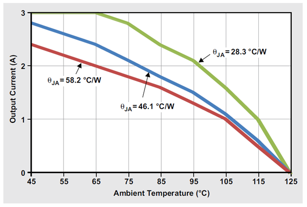
 Figure 1 Derating Curve for the a
MicroSiP Power Module
Figure 1 Derating Curve for the a
MicroSiP Power ModuleActually, each curve in Figure 1 uses the same TPS82130 power module under the same operating conditions. Only the printed circuit board (PCB) layout and airflow have changed. You, the designer, choose which derating curve you get. This brings to light a key truth about power modules: their thermal performance, and thus their derating, is highly dependent on the application and usage of the device, which includes the PCB layout and system variables such as airflow.
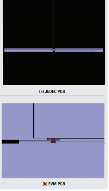
Specifically, the red curve in Figure 1 is generated with the standard Joint Electronic Devices Engineering Council (JEDEC) PCB design. While JEDEC’s board definition is used to generate most thermal tables in device data sheets, the JEDEC board is not a very realistic type of board for final applications.
How to Optimize Your Power Module's Thermal Performance.
 Figure 2 The JEDEC PCB Uses Very Thin
Amounts of Copper Connecting to the Device’s Pins
Figure 2 The JEDEC PCB Uses Very Thin
Amounts of Copper Connecting to the Device’s PinsConclusion
| JEDEC | EVM | |||||
|---|---|---|---|---|---|---|
| Vias | 3 | 0 | 3 | 3 | 6 | 6 |
| Layers | 4 | 4 | 4 | 6 | 4 | 4 |
| 200 linear-feet-per-minute (LFM) airflow | No | No | No | No | No | Yes |
|
ΘJA (˚C/W) |
58.2 | 51.4 | 46.1 | 44.6 | 43.8 | 28.3 |
| Module temperature (˚C) at full load | 118.7 | 107.8 | 99.22 | 96.8 | 95.5 | 70.6 |