SSZT907 november 2017
When you test the video feed from your newly designed camera module, have you ever noticed slow-moving bars, discoloration or flickering in your video, or no video at all?
There can be many different reasons for video issues like these: switching noise from a switcher, voltage ripple during frames or rows, elevated system temperature, or even damage to an imager. In this blog post, I will address three design techniques that reduce voltage ripple caused by load steps from an imager and image signal processor (ISP) using the Automotive 1MP Camera Module Reference Design with YUV422 Output, FPD-Link III and Power Over Coax and Automotive 1MP Camera Module Reference Design with YUV422, FPD-Link III and 4V-36V Power Over Coax. Below is the block diagram for the 4-36V Power Over Coax camera module reference design. Previous design approaches for camera modules only included considerations for just the imager. However, introducing an ISP created a new set of challenges.
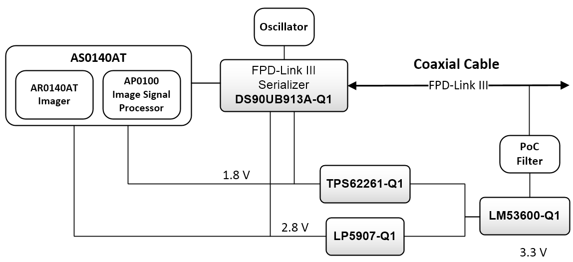 Figure 1 Automotive 4V-36V Power over
Coax Reference Design Block Diagram
Figure 1 Automotive 4V-36V Power over
Coax Reference Design Block DiagramBecause of frame and row transitions, the dynamic loading of both the imager and ISP can create considerable voltage ripple on the analog rails. For example, during the transition to a new frame or row, the current draw resembles a load step, requiring 100-200mA during a row or frame and 10-20mA during row or frame dead time. Figure 2 shows the actual 2.8V rail load current waveform in yellow, and the 2.8V rail voltage ripple in pink. Figure 2 was taken on the first revision. I had to address this unexpected ripple.
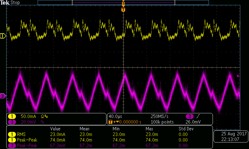 Figure 2 60mVP-P Voltage
Ripple Caused by the Dynamic Loading of a 2.8V Rail
Figure 2 60mVP-P Voltage
Ripple Caused by the Dynamic Loading of a 2.8V RailFigure 3 and Figure 4 are oscilloscope screenshots that show the fast Fourier transform (FFT) of the load-current waveforms for 2.8V and 1.8V rails, respectively. I measured the load current waveforms by replacing ferrite beads between the supply and rail decoupling capacitors with a loop of wire, and then placing a grounded current probe on that wire.
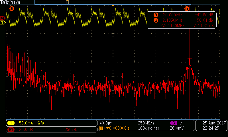 Figure 3 FFT of a 2.8V Load
Current
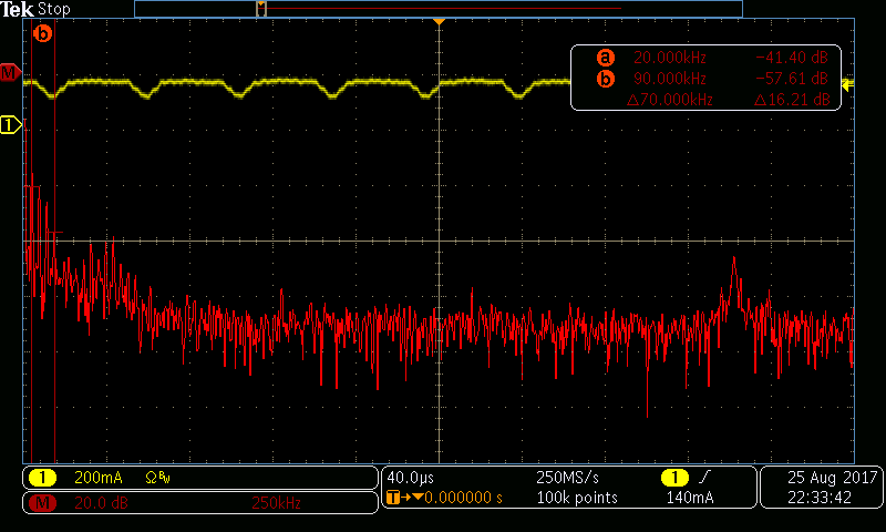 Figure 4 FFT of a 1.8V Load
Current
Figure 4 FFT of a 1.8V Load
CurrentNote the differences in magnitude of frequency content close to DC, spanning up into the 400kHz range, between the 2.8V load-current waveform in Figure 3 and the 1.8V load-current waveform in Figure 4. The spike around 2MHz comes from the switching frequency of the buck converters.
The first approach I’ll discuss will be the use of ferrite beads. While you probably already know that ferrite beads are used to isolate noise or reduce high frequency noise, there are some cases where ferrite beads between the voltage rail and supply can exacerbate voltage ripple, in some cases doubling the voltage ripple at the imager.
Row and frame rates occur at frequencies closer to DC (22.4-44.8kHz, 30-60Hz typical, respectively), and the loading within each row and frame requires fairly dynamic currents. These load steps occur so quickly that practical power supplies cannot recover before the next load step. Even in testing, common programmable load test equipment can only provide load steps as fast as 15kHz. The originally recommended ferrite bead had a considerable DC resistance of 500mΩ. The dynamic load current through this resistance will create voltage that is closely predicted by V= IR, and may resemble something like Figure 5. If a ferrite bead is used, it should have low DCR to most effectively reduce this low frequency voltage ripple while mitigating high frequency noise as originally intended.
Figure 5 and Figure 6 are oscilloscope shots that show the effect of ferrite-bead removal on the 2.8V analog rail.
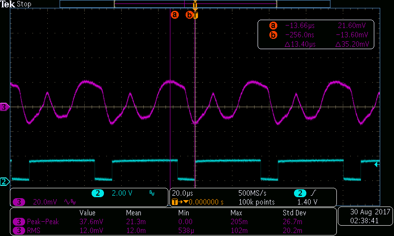 Figure 5 2.8V Voltage Ripple with
Ferrite Bead – 35.2mVP-P
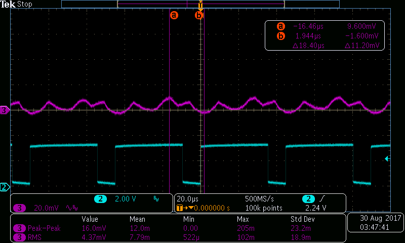 Figure 6 2.8V Voltage Ripple without
Ferrite Bead – 11.2mVP-P
Figure 6 2.8V Voltage Ripple without
Ferrite Bead – 11.2mVP-PThe second approach is to ensure tight current loops between the power supplies and the imager rails, which reduces ripple by minimizing current-loop and parasitic trace inductance.
In order to benefit from this approach, place supplies as close to the imager rails as practically possible. Unless vias for both power and ground paths are in close proximity and viewed as a pair, the loop inductance can be much higher and introduce a larger-than-normal voltage ripple. Figure 7 shows the recommended vias in the PCB view of the camera module design. These vias are circled.
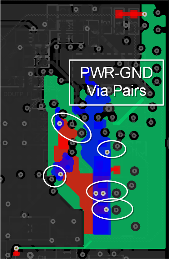 Figure 7 Example of Power-ground via
Pairs from the Automotive 4V-36V Power over Coax Reference Design
Figure 7 Example of Power-ground via
Pairs from the Automotive 4V-36V Power over Coax Reference DesignWhen mechanical housings or form-factor requirements limit power-supply placement, carefully consider the layer stack up. Placing the load and power layers close together will keep the current loop as small as possible in the z-direction between load and supply.
Like tight current loops, using power and ground planes also reduces current-loop inductance and parasitics. As camera modules get increasingly smaller, you must give power planes extra attention. When routing the many video and control signals through vias, PCB editing software automatically removes copper from power or ground planes in order to make room for these vias. Staggering signal vias and reducing the hole diameter automatically created by the software can drastically improve the continuity of power and ground planes, and in turn reduce loop inductance. Figure 8 and Figure 9 show the early ground plane compared to the improved ground plane.
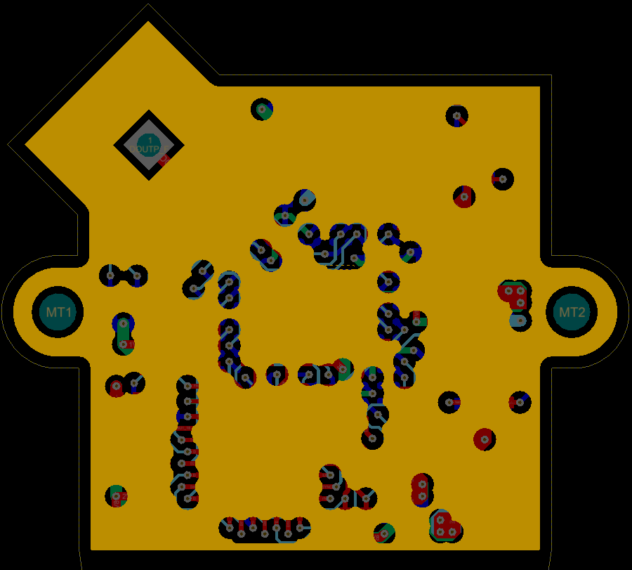 Figure 8 Revision 1 GND Layer
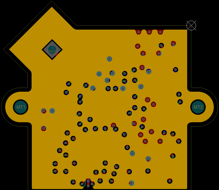 Figure 9 Final Revision GND
Layer
Figure 9 Final Revision GND
LayerThe third and final approach is to optimize decoupling capacitors. For imager decoupling, I recommend using larger bulk capacitors such as 10µF, 22µF or 47µF, as these have the lowest impedance around frequencies shown in Figure 3 and Figure 4 with the FFT. I tested different decoupling capacitor combinations for these designs, but they were not implemented in the final revisions.
Figure 10 and Figure 11 show the voltage ripple on the 2.8V rails for the final revisions of both the Automotive Power Over Coax and Automotive 4V-36V Power Over Coax reference designs.
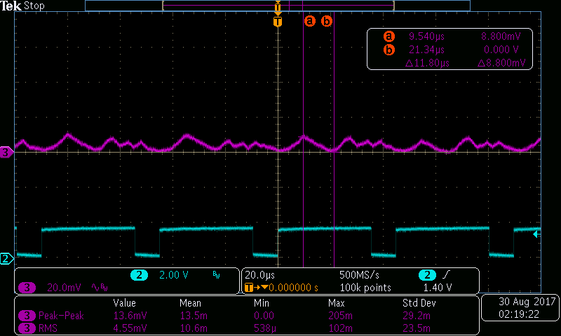 Figure 10 Automotive Power over Coax
Reference Design Final 2.8V Voltage Ripple
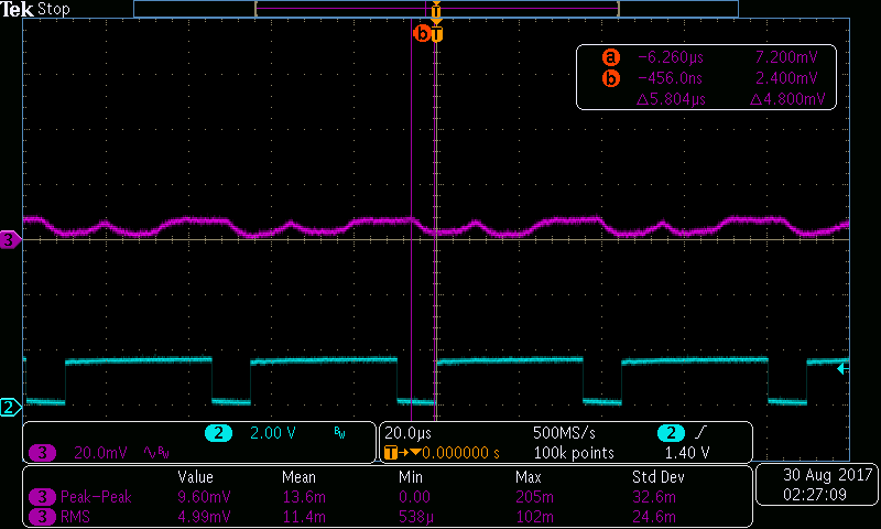 Figure 11 Automotive 4V-36V Power over
Coax Reference Design Final 2.8V Voltage Ripple
Figure 11 Automotive 4V-36V Power over
Coax Reference Design Final 2.8V Voltage RippleThe voltage ripple dropped from roughly 40-60mVP-P to 5-8mVP-P, improving by a factor of 8 to 10 by using these design techniques:
- Ferrite bead DCR reduction or removal
- Current loop reduction between dynamic load and supply
- Decoupling capacitor optimization
Additional Resources:
- Learn more about TI’s ADAS reference designs
- Learn more about automotive rear view camera module with integrated image processing
- Learn more about automotive front camera module with integrated image processing
- Learn more about FPD-Link™ in the Learning Center