SSZTA58 May 2017 TLV717P , TPS7A16
The key goal of DC power management is to provide a regulated, steady voltage for the slew of electronic content present in any system. This is particularly true for low-dropout regulators (LDOs), as they can achieve a regulated voltage while supplying current as needed.
There are external conditions and scenarios where an LDO might experience an unexpected high current draw. This high current will harm most electronic systems as well as the host power-management circuit if the current is transmitted to the other electronics being powered. Selecting an LDO with internal protection from short circuits and current limiting can help prevent this harmful effect and provide additional protection when designing the overall power management.
What Is Current Limiting/how Does It Work?
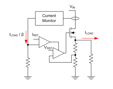
 Figure 1 A Current-limiting Internal LDO Structure
Brick-wall Current Limiting
 Figure 2 (1)
The pass transistor will continue this operation and dissipate power, as long as the thermal resistance (θJA) allows for healthy power dissipation where the junction temperature is within acceptable limits (TJ < 125°C). Once VOUT goes too low and the thermal limit is reached, thermal shutdown will turn off the device in order to protect it from permanent damage. Once the device has cooled, it will turn back on and regulation can proceed. This is particularly important in cases where a short circuit may present itself, as the LDO will proceed to regulate VOUT to 0V.
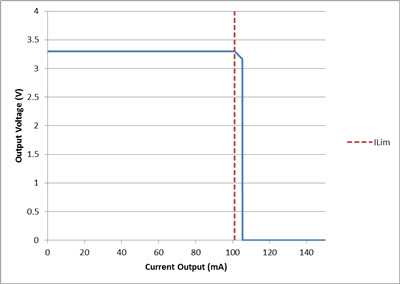
For example, TI’s TPS7A16 can limit high current outputs in wide voltage conditions. Figure 3 shows an example behavior of the current-limiting function in 30V input conditions. As you can see, once the current limit is surpassed, the LDO continues to supply at the limit, but it will no longer regulate VOUT to 3.3V. Once the thermal limit is surpassed at 105mA, thermal shutdown kicks in.
This current-limiting function is helpful for charging nickel-cadmium and nickel-metal hydride single-cell batteries, as both require a constant current supply. An LDO like the TPS7A16 can help maintain a constant current at the limit (ILIMIT) as the battery voltage changes while the battery is charging.
 Figure 3 TPS7A16 Brick-wall Current Limiting (30VIN, 3.3VVIN, VSON at 25°C)
Foldback Current Limit
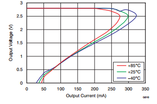
 Figure 4 TLV717P Output Current Limit vs. VOUT
Whenever harmful conditions may be present such as short circuits or overloading, it is important to prevent the transmission of this effect to other sensitive electronics. Protected LDOs can provide a wide range of functionality that can make any design much more robust. Read more blog posts on the basics of LDO design.