SSZTBZ6 November 2015 LM5021 , UCC28881
As I mentioned in my last blog, a cascode MOSFET configuration provides a low-cost alternative for high-voltage applications such as smart meters and motor drives. To further understand how a cascode MOSFET configuration works in high-voltage converters, Figure 1 shows a MOSFET modeled by a switch in parallel with a diode and a capacitor,. In addition to the switch, diode and paralleled capacitor, you must also consider the gate-to-source capacitance, Cg, of the top-side MOSFET.
In this blog post, I will discuss two possible operational conditions when using a cascode MOSFET configuration: Vin < VZc and Vin ≥ VZc, where VZc is the clamping voltage of the Zener diode ZC.
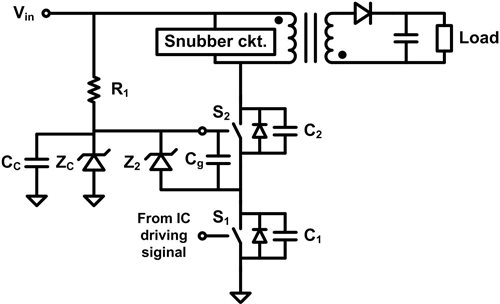 Figure 1 Flyback Converter in a Cascode
MOSFET Configuration
Figure 1 Flyback Converter in a Cascode
MOSFET ConfigurationVin < VZc
When the converter first powers up, capacitor CC will be charged to Vin through R1. Once the controller bias voltage is charged above the undervoltage lockout (UVLO) threshold, switch S1 turns on. As shown in Figure 2, when S1 turns on, the energy in CC transfers to Cg and leads to voltage increases on Cg. In order to turn on S2, the clamping voltage of Z2 needs to be set higher than the gate-to-source threshold voltage (Vgs(th)) of the top-side MOSFET. It is important to have enough energy in Cg to keep the top-side MOSFET turned on during the entire on state after the bottom-side MOSFET turns on. In other words, CC can’t be too small. Sometimes, the parasitic capacitance of ZC might not be enough and will require an external capacitor in parallel with ZC.
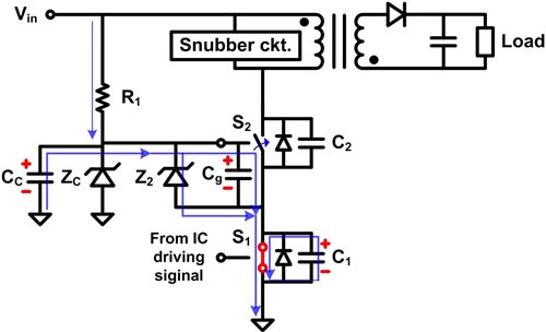 Figure 2 MOSFET Turned-on Transient
When the MOSFET on the bottom side turns off (Figure 3), the current from the transformer quickly charges C1. Cg discharges and energy goes back to CC again. Once Cg discharges to a voltage level lower than Vgs(th), S2 turns off and C2 charges up.
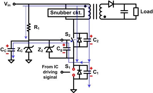 Figure 3 MOSFET Turned-off Transient (vin < VZc)
Vin ≥ VZc
The current-flow directions during the low-side MOSFET turned-on transient when Vin ≥ VZc are exactly the same as when Vin < VZc. During low-side MOSFET turned-off transient, transformer current discharges Cg and then flows through CC and ZC, as shown in Figure 4. In this transient, ZC acts as a snubber and clamps the low-side MOSFET voltage to VZc + VF_Z2, where VF_Z2 is the Zener forward voltage drop of Z2.
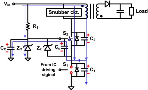 Figure 4 MOSFET Turned-off Transient (vin ≥ VZc)
The longer turn-off delay time S2 has after S1 has already turned off, the higher current flows through S2 to ZC, which might lead to a thermal issue for ZC. Figure 5 below shows a turn-off transient example. As you can see, S2 is starting to turn off after S1 is fully turned off. In the transient, S1 is already off and S2 is turning on. A surge current flows through ZC and this causes a thermal issue with Zener diode ZC.
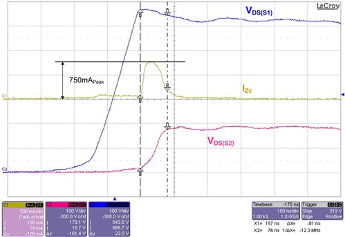 Figure 5 Waveforms During MOSFET Turned-off Transient with a Longer Turn-off Delay Time (vin ≥ VZc)
If the turn-off delay time between S1 and S2 can be minimized by using MOSFETs with better transient characteristics (like the example in Figure 6), the current going to ZC can also be minimized, and reducing the temperature rise of ZC.
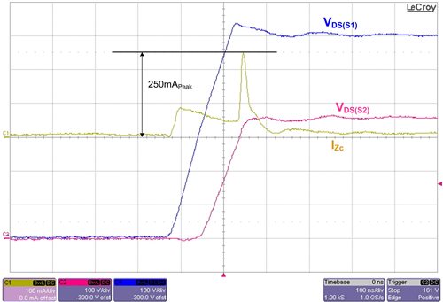 Figure 6 Waveforms During Low-side MOSFET Turned-off Transient with a Shorter Turn-off Delay Time (vin ≥ VZc)
Many components go into designing high voltage converters with a cascode MOSFET configuration, but mastering the key operations with carefully circuit parameter selection allows for a low cost alternative for high-voltage applications.
Additional Resources
- Discover TI’s Power Tips blog series on Power House.
- Check out the following TI Designs reference design, which use a cascode MOSFET configuration