SSZTC28 october 2015 UCC27201A-Q1 , UCC27282-Q1
In Peter Fundaro’s previous post on 48V automotive systems, he introduced a power-inverter system architecture and configuration as well as the design considerations for MOSFETs and high-side/low-side gate drivers. Integrating all of these parts into a robust system and implementing it efficiently requires a thorough understanding of the loss mechanism of the system, and how to balance the trade-offs. In this post, I will discuss the loss mechanism in a 48V system, the design trade-offs of high- and low-side gate drivers, parasitic inductances/capacitances, and printed circuit board (PCB) layout considerations.
Take a look at the power stage of the 48V inverter system shown in Figure 1. It includes three MOSFET half bridges and corresponding high- and low-side gate drivers.
 Figure 1 Power Stage of a 48V System
Inverter
Figure 1 Power Stage of a 48V System
InverterFigure 2 shows a simplified circuit featuring the configuration of the high- and low-side gate driver and the MOSFET’s half bridge for one phase leg in Figure 1.The loss on this power stage dominates the power loss for the whole 48V inverter system, which includes switching loss and conduction loss. Peter’s post discussed the trade-off between conduction loss and switching loss. Given selected power MOSFETs and system power ratings, the conduction loss is pre-determined, since the current-ripple-dependent root-mean-square (RMS) current is pre-determined by the motor. Switching loss is dependent on the gate-driver design, however.
 Figure 2 Simplified Circuit for One
Phase Leg
Figure 2 Simplified Circuit for One
Phase LegFigure 3 shows the simplified piecewise linear switching-loss mechanism for MOSFETs with turn-on, turn-off and turn-on with reverse recovery. The overlapped VDS and ID, t1~t3 shown in Figure 3 generates switching energy and is represented by the integration of the product of VDS and ID, expressed as Equation 1.
 Figure 3 Simplified Piecewise Linear
Switching-loss Mechanism
Figure 3 Simplified Piecewise Linear
Switching-loss Mechanism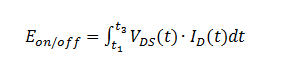
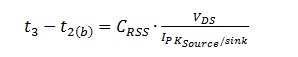
Given a certain switching voltage and current, the switching energy is decided by the driver’s output peak source/sink current, IPK_Source/Sink, and the parasitic capacitance of one MOSFET decides the switching period. Equation 2 estimates the interval from t2(b) to t3:
Therefore, the gate peak-current driving capability is very critical to switching loss. Ideally, the higher the gate driver’s current capability, the smaller the loss. But unfortunately, a higher driving current will bring high dv/dt and di/dt and its unfavorable influence on system operation through parasitics. Figure 4 shows a bootstrap high- and low-side driver-application circuit design considering parasitics. Looking at Figure 4, with high dv/dt on the switch node, SW, more noise will be coupled to the primary side through the parasitic capacitance, CIO, in the bootstrap level shifter and junction capacitance of the bootstrap diode (see red shaded path with arrow).
Plus, higher di/dt on the device will cause more noise on the gate-driver loop through the common source inductance, LSS. The voltage drop will always contradict the gate-drive signal by slowing down the driving capability. The voltage drop will also cause significant ringing on the MOSFET’s gate-source pin or over/undershoot on the MOSFET and gate-driver output pin, leading to reliability issues or even damage to the device under test (DUT).
 Figure 4 Gate-drive Circuit Considering
Parasitics
Figure 4 Gate-drive Circuit Considering
ParasiticsConsidering two active MOSFETs in each phase leg for the 48V system, hard switching and reverse-recovery loss will dramatically increase the switching loss; the major reason is because of the lousy parasitic body diode of the MOSFETs. Importantly, di/dt has a very strong influence on reverse-recovery charge and performance. Higher di/dt leads to a higher reverse-recovery charge and current, which could be 5 to 10 times higher than the rated switching current.
Figure 3(c) shows the piecewise linear turn-on waveform considering reverse recovery. Figure 5 shows an example turn-on/turn-off experimental waveform. As you can see from Figure 5(b), there is significant reverse-recovery current when the switch has a hard turn-on with the parasitic body diode, which not only causes significant current stress and large oscillation on the gate-drive voltage for the switch, but also significantly increases the switching loss. Other unfavorable effects would be electromagnetic interference (EMI), control ground noise, device/driver damage and low reliability.
 Figure 5 Hard Switching Turn-on/off
Waveform
Figure 5 Hard Switching Turn-on/off
WaveformTherefore, proper gate resistance should be sized considering the minimized switching loss, as well as maintaining acceptable dv/dt, di/dt and reverse-recovery performance. One solution to this trade-off is to split the turn-on/turn-off on the gate-driver design (see Figure 4, which has different RON and ROFF). A smaller ROFF will decrease turn-off loss (make sure that the dv/dt is not over the specifications for the driver) and RON can control the reverse-recovery performance to an acceptable level.
Figure 6 offers clues about gate-drive resistance and its influence on reverse-recovery current, Irr. Achieving a clean and sharp waveform on the gate drive and minimizing the VDS voltage spikes on the MOSFET requires careful layout. I recommend minimizing the loop inductance for the gate-driver loop, and minimizing the coupling common-source inductance, LSS.
For a 48V system application, TI’s UCC27282-Q1 offers 120V, ±3A driving capability, which gives you more flexibility to minimize the switching loss. More importantly, its state-of-the-art voltage-slew rate on the HS pin, 50V/ns, combines with a maximum negative voltage on the HS pin of -14V (repetitive pulse), enabling you to further push the driver’s peak-current capability while still maintaining robustness. The UCC27282-Q1 also integrates a 120V bootstrap diode with a 0.55V forward-voltage drop and 1.5Ω of dynamic resistance for a reliable charge transfer to the bootstrap capacitor.
 Figure 6 Peak Reverse-recovery Current
versus Turn-on Resistance and Id
Figure 6 Peak Reverse-recovery Current
versus Turn-on Resistance and IdAdditional Resources
- Check out TI’s 120V boot 3A peak high-frequency high-side/low-side driver.
- Read Laszlo Balogh’s article on, “Design And Application Guide For High Speed MOSFET Gate Drive Circuits”