SWRU382E July 2014 – November 2023 WL1807MOD , WL1837MOD
- 1
- WL1837MODCOM8I WLAN MIMO and Bluetooth Module Evaluation Board for TI Sitara Platform
- Trademarks
- Warning
- 1Overview
- 2Board Pin Assignment
- 3Electrical Characteristics
- 4Approved Antenna Types and Maximum Gain Values
- 5Antenna Characteristics
- 6Circuit Design
- 7Layout Guidelines
- 8Ordering Information
- 9Revision History
7.1 Board Layout
Figure 7-1 through Figure 7-4 show the four layers of the WL1837MODCOM8I EVB.
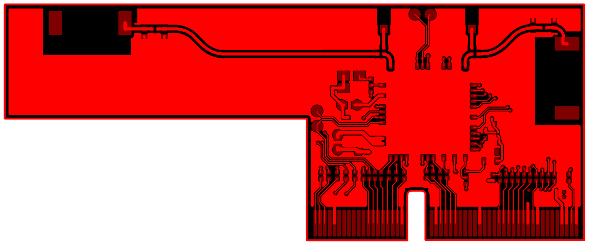 Figure 7-1 WL1837MODCOM8I Layer 1 Layout
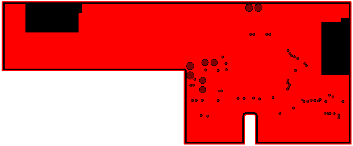 Figure 7-2 WL1837MODCOM8I Layer 2 Layout
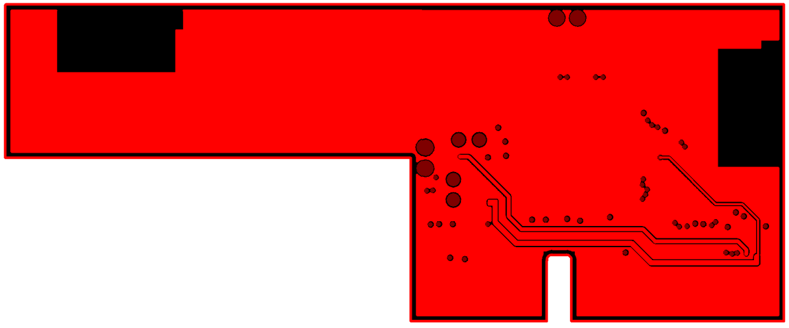 Figure 7-3 WL1837MODCOM8I Layer 3 Layout
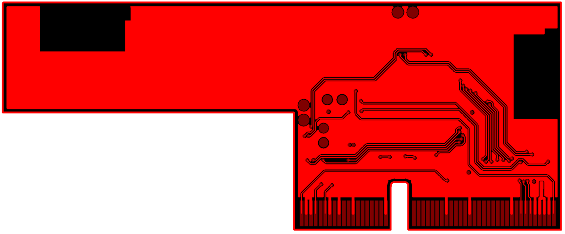 Figure 7-4 WL1837MODCOM8I Layer 4 Layout
Figure 7-5 and Figure 7-6 show instances of good layout practices.
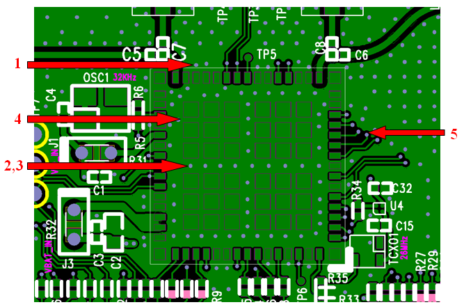 Figure 7-5 Module
Layout Guidelines (Top Layer)
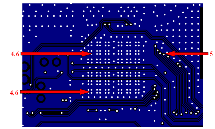 Figure 7-6 Module
Layout Guidelines (Bottom Layer)
Figure 7-6 Module
Layout Guidelines (Bottom Layer)Table 7-1 describes the guidelines corresponding to the reference numbers in Figure 7-5 and Figure 7-6.
| Reference | Guideline Description |
|---|---|
| 1 | Keep the proximity of ground vias close to the pad. |
| 2 | Do not run signal traces underneath the module on the layer where the module is mounted. |
| 3 | Have a complete ground pour in layer 2 for thermal dissipation. |
| 4 | Make sure to have a solid ground plane and ground vias under the module for stable system and thermal dissipation. |
| 5 | Increase ground pour in the first layer and have all traces from the first layer on the inner layers, if possible. |
| 6 | Signal traces can be run on a third layer under the solid ground layer and the module mounting layer. |
Figure 7-7 shows the trace design for the PCB. TI recommends using a 50-Ω impedance match on the trace to the antenna and 50-Ω traces for the PCB layout.
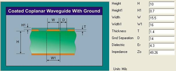 Figure 7-7 Trace
Design for the PCB Layout
Figure 7-7 Trace
Design for the PCB LayoutFigure 7-8 shows layer 1 with the trace to the antenna over ground layer 2.
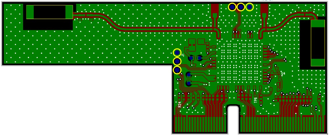 Figure 7-8 Layer 1
Combined With Layer 2
Figure 7-8 Layer 1
Combined With Layer 2Figure 7-9 and Figure 7-10 show instances of good layout practices for the antenna and RF trace routing.
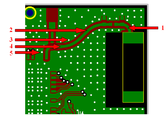 Figure 7-9 Top Layer
– Antenna and RF Trace Routing Layout Guidelines
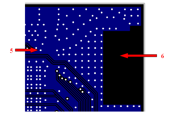 Figure 7-10 Bottom
Layer – Antenna and RF Trace Routing Layout Guidelines
Figure 7-10 Bottom
Layer – Antenna and RF Trace Routing Layout GuidelinesTable 7-2 describes the guidelines corresponding to the reference numbers in Figure 7-9 and Figure 7-10.
| Reference | Guideline Description |
|---|---|
| 1 | The RF trace antenna feed must be as short as possible beyond the ground reference. At this point, the trace starts to radiate. |
| 2 | RF trace bends must be gradual with an approximate maximum bend of 45 degrees with trace mitered. RF traces must not have sharp corners. |
| 3 | RF traces must have via stitching on the ground plane beside the RF trace on both sides. |
| 4 | RF traces must have constant impedance (microstrip transmission line). |
| 5 | For best results, the RF trace ground layer must be the ground layer immediately below the RF trace. The ground layer must be solid. |
| 6 | There must be no traces or ground under the antenna section. |
Figure 7-11 shows the MIMO antenna spacing. The distance between ANT1 and ANT2 must be greater than half the wavelength (62.5 mm at 2.4 GHz).
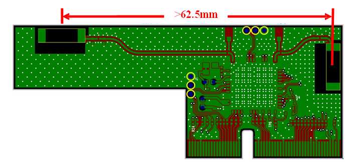 Figure 7-11 MIMO
Antenna Spacing
Figure 7-11 MIMO
Antenna SpacingFollow these supply routing guidelines:
- For power supply routing, the power trace for VBAT must be at least 40-mil wide.
- The 1.8-V trace must be at least 18-mil wide.
- Make VBAT traces as wide as possible to make sure that reduced inductance and trace resistance.
- If possible, then shield VBAT traces with ground above, below, and beside the traces.
Follow these digital-signal routing guidelines:
- Route SDIO signal traces (CLK, CMD, D0, D1, D2, and D3) in parallel to each other and as short as possible (less than 12 cm). In addition, each trace must be the same length. Make sure there is enough space between traces (greater than 1.5 times the trace width or ground) to verify signal quality, especially for the SDIO_CLK trace. Remember to keep these traces away from the other digital or analog signal traces. TI recommends adding ground shielding around these buses.
- Digital clock signals (SDIO clock, PCM clock, and so on) are a source of noise. Keep the traces of these signals as short as possible. Whenever possible, maintain a clearance around these signals.