TIDA035 October 2020
4.1 Input offset voltage
The output of an ideal op-amp should be zero if the input voltage difference is zero. But the mismatch of differential input transistors of real op-amps causes the output to be zero at a non-zero value of differential input, which is known as input offset voltage.
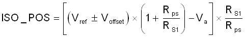
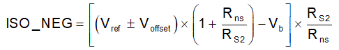
It is assumed that the inverting input (–) voltage of the op-amp is equal to non-inverting input (+) in the above calculation. And the non-inverting input (+) is connected to the voltage reference Vref.
Once the input offset voltage is considered between the non-inverting input (+) and the inverting input (–), ISO_POS and ISO_NEG can take into account the input offset voltage from Equation 2 and Equation 5 respectively.