TIDUEO0C July 2019 – March 2021
- Description
- Resources
- Features
- Applications
- 5
- 1System Description
-
2System Overview
- 2.1 Block Diagram
- 2.2 Design Considerations
- 2.3
Highlighted Products
- 2.3.1 TPS63900: 1.8V-5.5 VIN Buck-Boost Converter With 75-nA Ultra-low Quiescent Current and 400-mA Output Current
- 2.3.2 TPS610995: 0.7 VIN Synchronous Boost Converter With 400-nA Ultra-low Quiescent Current and 1-A Peak Current
- 2.3.3 TPS62840: 750-mA Synchronous Step-Down Converter With Ultra-low Quiescent Current Consumption
- 2.4 System Design Theory
- 3Hardware, Software, Testing Requirements, and Test Results
- 4Design Files
- 5Software Files
- 6Related Documentation
- 7Terminology
- 8About the Author
- 9Revision History
2.4.2.1 Resistor Values Calculation for the two Current Ranges
The following explains how designers can customize the two current ranges to support many other battery-powered IoT applications in only two steps:
- Changing (if necessary) the values of R32 and R33 in the TIDA-01546 system monitoring subsystem schematics (see Figure 2-5)
- Software modifications for the high- and low-threshold registers of the ADS7142 device
The default resistor values for R32 = 6.8 kΩ and R33 = 0.1 Ω define the ranges 0–10 µA and 0–476 mA and achieve sufficient accuracy and resolution in each of these ranges. Select the resistors based on the load profile of the application. Note that in many cases, there are more than two current ranges for the load profile, so some simplification for this selection by the designer is needed.
Splitting the two ranges enables accurate measurement of both very low currents down to 300 nA (see the Battery and System Health Monitoring of Battery-Powered Smart Flow Meters Reference Design Guide) but also six orders of magnitude higher currents of up to 476 mA.
Only R32 = 6800 Ω is used when the system has settled after a possible load profile transition and operates in the 0–10 µA range, which is usually the case for the majority of the run time for many smart flow meters.
The system monitoring with the ADS7142 device is done by continuously comparing the current drawn by the application to the high and low thresholds and by raising an alarm through the ALERT pin to the TM4C Host MCU, if one of those is crossed.
 Figure 2-5 Dual Shunt for System Health Monitoring Subsystem in TIDA-01546
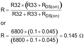
When the current rises above the programmed high-threshold level, the ALERT high event is triggered and the TM4C MCU gets an interrupt. Only if the system is already operating in the low-current range, the host switches on the CSD13383F4 FemtoFET™ device, which enables the current flow through R33. Thus, the overall resistance is now R32 || (R33 + the CSD RDS(on) ), where RDS(on) is assumed to be 45 mΩ at 3.3 V, based on the existing data sheet values.
The high threshold ALERT is re-triggered at the next data conversion, if the PRE_ALT_MAX_EVENT_COUNT is set to 0, but the TIDA-01546 firmware for the host MCU ignores it, if the device is already in the high-current range.
Vice versa, when the current drops back to low-current range, the ALERT pin is set by the low threshold and the MCU reads out which threshold set the alarm and switches the FemtoFET device off, which puts the system back to the initial condition.