SCES427B February 2003 – June 2014 SN74LVCR16245A
PRODUCTION DATA.
- 1 Features
- 2 Applications
- 3 Description
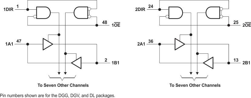
- 4 Simplified Schematic
- 5 Revision History
- 6 Pin Configuration and Functions
- 7 Specifications
- 8 Parameter Measurement Information
- 9 Detailed Description
- 10Application and Implementation
- 11Power Supply Recommendations
- 12Layout
- 13Device and Documentation Support
- 14Mechanical, Packaging, and Orderable Information
パッケージ・オプション
デバイスごとのパッケージ図は、PDF版データシートをご参照ください。
メカニカル・データ(パッケージ|ピン)
- DGG|48
- DL|48
- DGV|48
サーマルパッド・メカニカル・データ
発注情報
1 Features
- Member of the Texas Instruments
Widebus™ Family - Operates From 1.65 V to 3.6 V
- Inputs Accept Voltages to 5.5 V
- Max tpd of 4.8 ns at 3.3 V
- Typical VOLP (Output Ground Bounce)
<0.8 V at VCC = 3.3 V, TA = 25°C - Typical VOHV (Output VOH Undershoot)
>2 V at VCC = 3.3 V, TA = 25°C - Supports Mixed-Mode Signal Operation on All Ports (5-V Input/Output Voltage With 3.3-V VCC)
- All Inputs and Outputs Have Equivalent 26-Ω Series Resistors, So No External Resistors Are Required
- Ioff Supports Live Insertion, Partial-Power-Down Mode, and Back-Drive Protection
- Latch-Up Performance Exceeds 250 mA Per JESD 17
- ESD Protection Exceeds JESD 22
- 2000-V Human-Body Model (A114-A)
- 200-V Machine Model (A115-A)
3 Description
This 16-bit (dual-octal) noninverting bus transceiver is designed for 1.65-V to 3.6-V VCC operation.
The SN74LVCR16245A device is designed for asynchronous communication between data buses. All inputs and outputs have equivalent 26-Ω resistors that will slow the edges of the output and reduce switching noise caused by long capacitive etch runs or cables.
This device can be used as two 8-bit transceivers or one 16-bit transceiver. Active bus-hold circuitry holds unused or undriven data inputs at a valid logic state.
Device Information(1)
| PART NUMBER | PACKAGE | BODY SIZE (NOM) |
|---|---|---|
| SN74LVCR16245A | TSSOP (48) | 12.50 mm × 6.1 mm |
| TVSOP (48) | 9.70 mm × 4.40 mm | |
| SSOP (48) | 15.88 mm × 7.49 mm | |
| BGA MICROSTAR JUNIOR (56) | 7.00 mm × 4.50 mm |
- For all available packages, see the orderable addendum at the end of the datasheet.
4 Simplified Schematic