SBOU128B february 2013 – july 2023 INA231
- 1
- INA231EVM Evaluation Board and Software Tutorial
- Trademarks
- 1Overview
- 2INA231EVM Hardware
- 3INA231EVM (Rev A) Hardware Setup
- 4INA231EVM Software Setup
- 5INA231EVM Software Overview
- 6INA231EVM Documentation
- 7Revision History
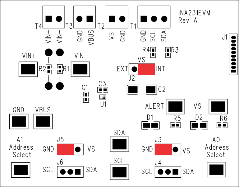
3.5 INA231EVM Default Jumper Settings
Figure 3-4 shows the default jumper configuration for the INA231EVM. In general, the jumper settings of the SM-USB-DIG Platform do not need to be changed. Users may want to change some of the jumpers on the INA231EVM board to match their specific configurations. For example, user can set a specific I2C address by configuring J3-J6.
 Figure 3-4 INA231EVM Default Jumper Settings
Typically, jumper 2 on the INA231EVM is always set to the INT position. When set to the INT position, the SM-USB-DIG Platform provides the supply for the INA231. When this jumper is set to the EXT position, an external supply voltage can be connected to terminal strip T2 to provide the supply for the INA231.
Jumpers 3 through 6 control the I2C address pins for the INA231. These jumpers can set the address for A0 and A1 to either supply, ground, SCL, or SDA. Make sure to only connect one jumper at a time for each address control. Failure to properly connect jumpers can cause shorts or interruptions in the communication lines. See also the INA231 data sheet.
Table 3-1 summarizes the function of the INA231 Test Board jumpers. For most applications, all jumpers should be left in the respective default configurations.
| JUMPER | DEFAULT |
PURPOSE |
|---|---|---|
| J2 | INT | This jumper selects whether the VS pin on the INA231 is connected to the VDUT signal generated from the SM-USB-DIG Platform or whether the digital supply pin is connected to terminal T2, allowing for an external supply to power the device. The default INT position connects the VS pin to the VDUT control signal. |
| J3/J4 | GND | This jumper selects the I2C A0 address selection for A0. |
| J5/J6 | GND | This jumper selects the I2C A1 address selection for A1. |