SLLA607 may 2023 MAX3222E , MAX3227E , MAX3243-EP , MAX3243E , SN75155 , TRS202E , TRS3122E , TRS3221E , TRS3223-Q1 , TRS3243E
3.3 Additional Features on Select TI RS-232 Transceivers
This section details a few features which are additional to RS-232 devices that are included on select TI RS-232 devices.
- Integrated Charge Pump
The vast majority of TI RS-232 devices use an integrated charge pump that requires external capacitors for charge pump operation. This allows the device to create the necessary RS-232 compliant output voltage swings from a single supply voltage (typically 3.3 V to 5 V). Some older devices do not have this feature and require dual supplies for RS-232 compliant operation.
- Slew Rate Control
One device, the SN55188, has an additional feature name slew rate control where there is a measured relationship between the output capacitor and the device slew rate. Most devices have a decrease in slew rate for an increase in output capacitance, the only difference is that this device gives a relationship to allow the customer to externally control the slew rate. For lower slew-rate requirements, picking a device with a lower data rate is generally a best practice.
- Power Down
Power down as a feature just allows the device to be controlled via enable signals, thus allowing the device to be enabled and disabled as needed throughout system operation. The power down feature allows for more flexible control over power usage in the system.
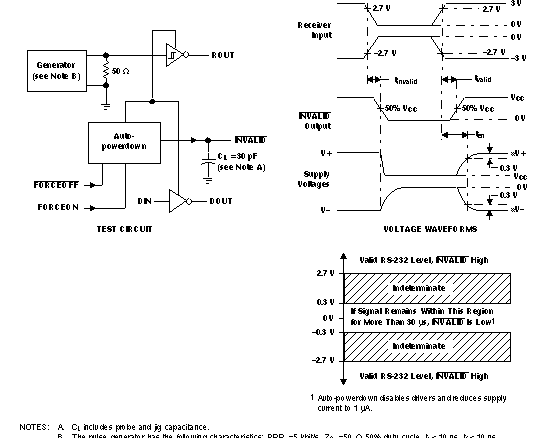
- Auto Power -Down and Auto Power-Down +
The Auto Power-Down and Auto Power-Down+ feature allows the device to go into a disabled state (charge pump inactive) after no transitions have occurred on the TX or RX inputs. The difference in delay time is typically 30 μs for Auto Power-Down Parts and 30 s for Auto Power-Down+ parts. These parts include a flag pin, INVALID, that goes low when the data on the RX bus is not within the valid range.

Figure 3-4 Auto-Power-Down Test Setup Example From TRSF3243E Data Sheet