SLLU320 November 2020 TRS3232E , TRSF3232E
4.1 Schematic
The schematic is shown in Figure 4-1. The function of each jumper and test point is listed in Table 4-1.
 Figure 4-1 TRS3232RGTEVM
schematic
Figure 4-1 TRS3232RGTEVM
schematic| Connection | Type | Description |
|---|---|---|
| J1 | 9-pin connector | Female DB9 connector to connect to PC |
| J2 | 16-pin jumper | Used for supply and TTL signal |
| V+ | Test point | Charge pump positive output |
| V- | Test point | Charge pump negative output |
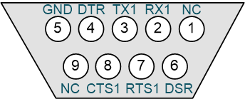
Power and logic signal go through the J1 connector. Table 4-2 lists each pin’s connection.
| Connection | Type | Description |
|---|---|---|
| 1 | NC | Not connected |
| 2 | Output | RX1, pin 12 of transceiver |
| 3 | Input | TX1, pin 11 of transceiver |
| 4 | Loopback | Connected to pin 6 |
| 5 | GND | Ground |
| 6 | Loopback | Connected to pin 4 |
| 7 | Input | RTS1, pin 6 of transceiver |
| 8 | Output | CST1, pin 5 of transceiver |
| 9 | NC | Not connected |
The female DB9 port (Figure 4-2) provides access to the TRS3232RGT device through a standard RS-232 pinout. The TRS3232RGT female port is DCE to mate with a computer's male DTE port. The pin names are counterintuitive on the DCE side. For example the RX pin on EVM is connected to a driver and TX connects to a receiver. The pin connection is listed in Table 4-3. The reason pins 4 and 6 are shorted together by a 0 Ω resistor is to loopback the unused handshaking lines.
 Figure 4-2 Female DB9 Connector Pinout
| Connection | Type | Description |
|---|---|---|
| 1 | GND | Ground |
| 2 | Input | CST2, pin 8 of transceiver |
| 3 | GND | Ground |
| 4 | Output | RTS2, pin 7 of transceiver |
| 5 | GND | Ground |
| 6 | Output | TX2, pin 10 of transceiver |
| 7 | GND | Ground |
| 8 | Input | RX2, pin 9 of transceiver |
| 9 | GND | Ground |
| 10 | GND | Ground |
| 11 | GND | Ground |
| 12 | GND | Ground |
| 13 | GND | Ground |
| 14 | Power | Ground |
| 15 | GND | Vcc |
| 16 | GND | Ground |