SLUA963B June 2020 – October 2022 UCC21710-Q1 , UCC21732-Q1 , UCC5870-Q1
- HEV/EV Traction Inverter Design Guide Using Isolated IGBT and SiC Gate Drivers
- 1Introduction
- 2HEV/EV Overview
-
3Design of HEV/EV Traction Inverter Drive Stage
- 3.1 Introduction to UCC217xx-Q1
- 3.2 Designing a Traction Inverter Drive System Using UCC217xx-Q1
- 3.3 Description of Protection Features
- 3.4 Protection Features of UCC217xx-Q1
- 3.5
UCC217xx-Q1 Protection and Monitoring Features Descriptions
- 3.5.1 Primary and Secondary Side UVLO and OVLO
- 3.5.2 Over-Current (OC) and Desaturation (DESAT) Detection
- 3.5.3 2-Level and Soft Turn-Off
- 3.5.4 Power Switch Gate Voltage (VGE/VGS) Monitoring
- 3.5.5 Power Switch Anti-Shoot-Through
- 3.5.6 Integrated Internal or External Miller Clamp
- 3.5.7 Isolated Analog-to-PWM Channel
- 3.5.8 Short-Circuit Clamping
- 3.5.9 Active Pulldown
- 3.6 Introduction to UCC5870-Q1
- 3.7 Designing a Traction Inverter Drive System Using UCC5870-Q1
- 3.8 Description of Protection Features
- 3.9 Protection Features of UCC5870-Q1
- 3.10
UCC5870-Q1 Protection and Monitoring Features Descriptions
- 3.10.1 Primary and Secondary Side UVLO and OVLO
- 3.10.2 Programmable Desaturation (DESAT) Detection and Over-Current (OC)
- 3.10.3 Adjustable 2-Level or Soft Turn-Off
- 3.10.4 Active High-Voltage Clamp
- 3.10.5 Power Switch Gate Voltage (VGE/VGS) Monitoring
- 3.10.6 Gate Threshold Voltage Monitor
- 3.10.7 Power Switch Anti-Shoot-Through
- 3.10.8 Active Short Circuit (ASC)
- 3.10.9 Integrated Internal or External Miller Clamp
- 3.10.10 Isolated Analog-to-Digital Converter
- 3.10.11 Short-Circuit Clamping
- 3.10.12 Active and Passive Pulldown
- 3.10.13 Thermal Shutdown and Temperature Warning of Driver IC
- 3.10.14 Clock Monitor and CRC
- 3.10.15 SPI and Register Data Protection
- 4Isolated Bias Supply Architecture
- 5Summary
- 6References
- 7Revision History
3.10.10.1 Temperature Monitoring of Power Transistor
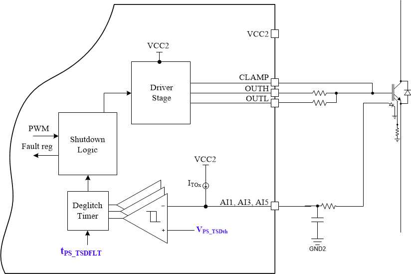
UCC5870-Q1 designates three AIx inputs (AI1, AI3, AI5) to support thermal diode sensing for up to three power transistors sharing the same ground reference. An example with a single thermal diode measurement is shown in Figure 3-28. The temperature protection is intended for power transistors with integrated temperature sensing diodes in order to monitor the junction temperature, which can be an indication for the controller to discontinue to operate the inverter or as a mode of failure. The AIx input provides a current that biases the integrated diode, and the voltage is monitored at the AIx input. The bias current can be enabled via SPI on one or all of the available AI pins. The temperature measurement is fed back into the ADC Data register, and a fault can also be configured for thermal shutdown (TSD) or thermal warning (TWN). The fault must exist for the deglitch time programmed before the fault is registered. The AIx pins can be enabled/disabled for temperature monitoring.
 Figure 3-28 Power switch temperature monitoring