SLUAA84A January 2021 – February 2022 BQ769142 , BQ76942 , BQ76952
8 Precharge and Predischarge for Low-Side FETs
The DDSG and DCHG outputs from the BQ769x2 combine the pre and main FET drive signals. If the designer wants precharge and or predischarge features, options include controlling the precharge or predischarge path from the host and using logic to inhibit the main FET driver when the presignal is applied. When using the host, the predischarge and precharge FET drivers may look like the main FET drivers described in earlier sections.
The precharge and predischarge outputs of the BQ769x2 are only referenced to the BAT voltage, a digital version referenced to VSS is not available. To use precharge and predischarge with a low-side implementation a circuit is needed to translate the voltage from the high side to the low-side FETs, an example is shown in Figure 8-1. P-channel signal FETs (Q28, Q29) are used to create a current which will flow to resistors (R51, R52) at the low side to turn on the FETs. Zener diodes (D8, D9) limit the voltage to the FET gates. Resistors in the drain path (R58, R60) drop the voltage to the Zener diodes limiting the drain current. If desired current could be limited by resistors in the source path. The current will vary across the battery voltage. The ratio of the resistors will determine the voltage for the gate of the low-side FET. The lower resistor must also be sized for turn off. Since PACK- can swing below GND and above PACK+, a diode (D7) is included to avoid current through these components.
The circuit in Figure 8-1 shows the signal translation circuit and precharge and predischarge FETs with 4.7-kΩ resistor-limited current paths for precharge and predischarge. This is not a complete system solution since logic is not included to allow these circuits to operate without the main FETs coming on at the same time. For example the main discharge FET would be enabled only when DDSG is active and the PDSGgate signal was low. The 4.7-kΩ resistors would also need to be adjusted for the desired current and allowed power in the design.
PDSG and PCHG are high impedance when off and pulled up by R55 and R57 for PDSG and R56 and R59 for PCHG. When PDSG and PCHG are active they pull to a voltage below the BAT level turning on Q28 and Q29 when appropriate. Connecting a scope probe to observe the PDSG and PCHG will generally pull down the signals and turn on the FETs, so these signals are not shown in the figures.
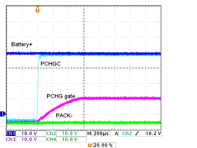
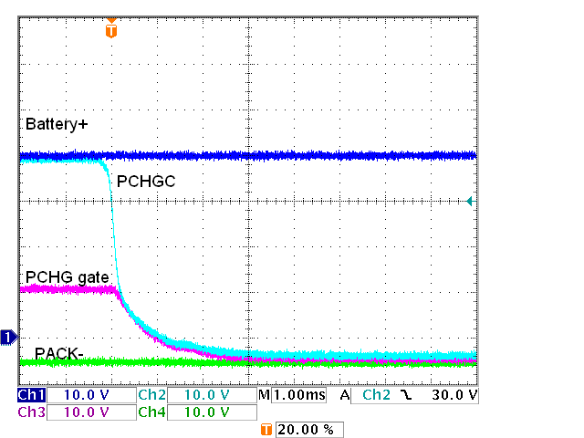
Basic operation of the level shift circuit is shown in Figure 8-2 and Figure 8-3 for the precharge circuit. In this circuit the level shift controls the FET directly. In these waveforms DCHG is disconnected so the main charge FET remains off and PACK- remains below GND. The PCHG signal is not shown on the waveform since loading of the scope probe will pull down the high impedance output turning on the external FET. When the CHG signal goes low, the P-channel FET pulls up the PCHGC signal to the battery voltage raising the PCHG gate signal to the limit of the Zener. Since the path is current limited the charger voltage remains below the battery- voltage, the probe reference in the figures. With large resistors to keep the current small switching is slow, most notably on turn off. With reduced current in the path the slow switching may be suitable for the FET although small FETs are often used due to the low current. Use an appropriate technique for your design. When generating a logic level signal to control the main charge driver remember the switching speed as well as the large voltage variation of PACK-. Use a path referenced to VSS for logic controls. Also when considering this circuit remember that PCHG and PDSG are referenced to the filtered BAT pin of the BQ769x2. If transients exist on the BAT+, consider filtering or limiting the VGS voltage for Q28 and Q29 and consider the effect of glitches on logic circuits.
 Figure 8-2 Precharge Turn On
 Figure 8-3 Precharge Turn
Off
Figure 8-3 Precharge Turn
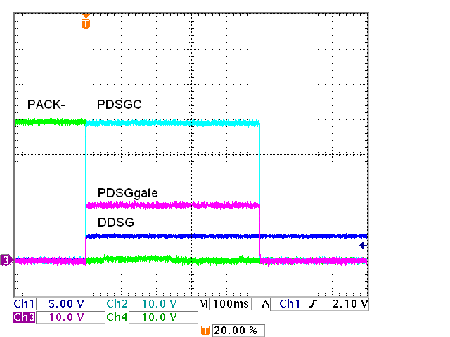
OffThe predischarge path shown in Figure 8-1 is referenced to the sense resistor which will not move much from VSS and is accommodated by the FET gate threshold. Figure 8-4 shows the limitation of the test circuit without the logic control of the main discharge FET. PDSG turns on the PDSGC signal which turns on the PDSGgate and the predischarge path, but DDSG also goes high which turns on the main discharge FET pulling PACK- down immediately rather than with the current limited predischarge path. The level change in PACK- while low is from a temporary turn off of the DCHG signal during the predischarge cycle. The main discharge FET would need to be disabled by logic during the predischarge time for predischarge to be effective.
 Figure 8-4 Predischarge Turn On