SLUSDG1C June 2020 – August 2022 BQ25792
PRODUCTION DATA
- 1 Features
- 2 Applications
- 3 Description
- 4 Revision History
- 5 Device Comparison
- 6 Description (continued)
- 7 Pin Configuration and Functions
- 8 Specifications
-
9 Detailed Description
- 9.1 Overview
- 9.2 Functional Block Diagram
- 9.3
Feature Description
- 9.3.1 Device Power-On-Reset
- 9.3.2 PROG Pin Configuration
- 9.3.3 Device Power Up from Battery without Input Source
- 9.3.4 Device Power Up from Input Source
- 9.3.5 Dual-Input Power Mux
- 9.3.6 Buck-Boost Converter Operation
- 9.3.7 USB On-The-Go (OTG)
- 9.3.8 Power Path Management
- 9.3.9 Battery Charging Management
- 9.3.10 Integrated 16-Bit ADC for Monitoring
- 9.3.11 Status Outputs ( STAT, and INT)
- 9.3.12 Ship FET Control
- 9.3.13 Protections
- 9.3.14 Serial Interface
- 9.4 Device Functional Modes
- 9.5 Register Map
- 10Application and Implementation
- 11Power Supply Recommendations
- 12Layout
- 13Device and Documentation Support
- 14Mechanical, Packaging, and Orderable Information
9.3.7.1 OTG Mode to Power External Devices
The device supports the OTG operation to deliver power from the battery to other external devices through the USB ports. The OTG voltage regulation is set in VOTG[10:0] register bits. The OTG current regulation is set in IOTG[6:0] register bits. To enable the OTG operation, the following conditions have to be valid:
- The battery voltage is higher than VBAT_OTG rising threshold, and not trigger the VBAT_OVP protection.
- The VBUS is below VVBUS_UVLO.
- The voltage at TS pin is within the range configured by BHOT and BCOLD register bits
The population of ACFET1-RBFET1 and ACFET2-RBFET2 as detected at POR affects the operation of the converter in OTG mode as summarized in Table 9-8.
| ACRB1_STAT | ACRB2_STAT | DIS_ACDRV | OTG BEHAVIOR |
|---|---|---|---|
| 0 | 0 | 0 | Converter starts 5 ms after EN_OTG = 1 |
| 0 | 1 | 0 | EN_OTG = 1 does not start converter until EN_ACDRV2 = 1 |
| 1 | 0 | 0 | EN_OTG = 1 does not start converter until EN_ACDRV1 = 1 |
| 1 | 1 | 0 | EN_OTG = 1 does not start converter until either EN_ACDRV1 = 1 or EN_ACDRV2 = 1 |
| X | X | 1 | Converter starts 5 ms after EN_OTG = 1 |
For swapping the OTG output from port 1 to port 2, assuming EN_ACDRV2 is already 0, the host has to set EN_ACDRV1 = 0 to turn off ACFET1_RBFET1 first, which causes the converter to stop switching and VBUS to drop below VBUS_PRESENT. The host then sets EN_ACDRV2 = 1, and the converter starts switching again and ACDRV2 turns on ACFET2-RBFET2, which allows VBUS to ramp up. The similar procedure can be applied to the case of swapping the OTG output from port 2 to port 1.
In OTG mode, the converter PFM operation can be disabled by setting PFM_OTG_DIS = 1 and the OOA can be disabled by setting DIS_OTG_OOA = 1.
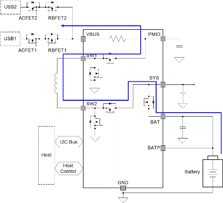
 Figure 9-5 The Simplified Application
Diagram for the OTG Mode Operation
Figure 9-5 The Simplified Application
Diagram for the OTG Mode OperationThe simplified application diagram for the OTG mode operation is shown in Figure 9-5, in which the power flow is illustrated by the blue arrows.
The charger regulates the battery discharging current in OTG mode. When IBAT rises higher than the IBAT_REG[1:0] register setting, the charger reduces the OTG output current and prioritizes the system load current if there is any. The IBAT_REG_STAT bit is set to 1 and an INT pulse is asserted, and if IBAT_REG_MASK = 0, the IBAT_REG_FLAG is set to 1. If the OTG output current is decreased to zero and the system load pulls even more current, the charger can no longer limit the battery discharging current.
When IBAT_REG[1:0] is set to 00, 01 or 10 (3A, 4A or 5A), there is a soft-start applied to the OTG ouput current. When IBAT_REG[1:0] is set to 11 (Disabled) no soft-start is applied.