SLUU182A January   2004  – March 2022 TPS5124


  1.   Trademarks
  2. 1Introduction
  3. 2Features
  4. 3Schematic
  5. 4Design Procedure
    1. 4.1 Frequency Setting
    2. 4.2 Inductance Value
    3. 4.3 Output Capacitors
    4. 4.4 Input Capacitors
      1. 4.4.1 Case One: D1, D2 < 0.5
      2. 4.4.2 Case Two: D2 < 0.5 < D1
    5. 4.5 Compensation Design
    6. 4.6 Current Limiting
    7. 4.7 Timer Latch
      1. 4.7.1 Undervoltage Protection
      2. 4.7.2 Short Circuit Protection
      3. 4.7.3 Overvoltage Protection
      4. 4.7.4 Disabling the Protection Function
        1. 4.7.4.1 Disabling the Overcurrent Protection
        2. 4.7.4.2 Disabling the Overvoltage Protection or Undervoltage Protection
  6. 5Test Results
    1. 5.1 Efficiency Curves
    2. 5.2 Typical Operating Waveform
    3. 5.3 Start-Up Waveform
    4. 5.4 Output Ripple Voltage and Load Transient
  7. 6Layout Guidelines
    1. 6.1 Low-Side MOSFET
    2. 6.2 Connections
    3. 6.3 Bypass Capacitor
    4. 6.4 Bootstrap Capacitor
    5. 6.5 Output Voltage
  8. 7PCB Layout
  9. 8List of Materials
  10. 9Revision History

Compensation Design

The following compensation loop design uses Channel 1 as example, but a design for Channel 2 follows the same rules.

The TPS5124 uses voltage-mode control method. A Type III compensation network, formed by R1, R2, R4, C14, C12, and C23, is used to ensure the stability. The L-C frequency of the power stage is around 5.4 kHz and the ESR zero is at 790 KHz due to the low ESR of the ceramic capacitors. An overall crossover frequency (f0db) of 30 kHz is chosen for reasonable transient response and stability. Both zeros (fZ1 and fZ2) from the compensator are set at 2.68 kHz. The two poles (fP1 and fP2) and are set at 150 kHz and 2 MHz. The frequency of poles and zeros are defined by the following equations.

Equation 11. f Z 1 =   1 2 π   × R 4   × C 14
Equation 12. f Z 2 =   1 2 π   × R 1   × C 12

where

  • R1 >> R2 is assumed.
Equation 13. f P 1 =   1 2 π   × R 4   × C 23
Equation 14. f P 2 =   1 2 π   × R 2   × C 12

where

  • C14 >> C23 is assumed.

The transfer function for the compensator is calculated as:
Equation 15. A s =   1 + s   × C 14   × R 2 × [ 1 + s   × C 12   × R 1 + R 2 ] s   × R 1   × C 14   × 1 + C 23 C 14 + s   × R 4   × C 23 × ( 1 + s   × R 2   × C 12 )  
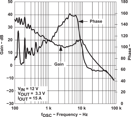
GUID-20220302-SS0I-CQCM-HFDS-NFZHJWBNWWMT-low.gifFigure 4-3 Gain and Phase vs Oscillator Frequency (Channel 1)
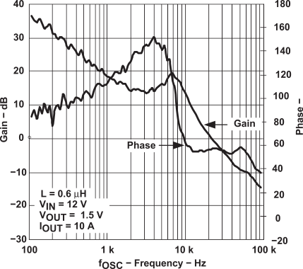
GUID-20220302-SS0I-JTC5-CFJV-CVZVWKTCDQNK-low.gifFigure 4-4 Gain and Phase vs Oscillator Frequency (Channel 2)

Figure 4-3 shows the closed loop gain and phase. For Channel 1, the overall crossover frequency is approximately 30 kHz and the phase margin is 58°. For Channel 2, the crossover frequency is approximately 23 kHz and phase margin is 55°.