SLUUCS3 February   2023 LM2105


  1.   Abstract
  2.   Trademarks
  3. Introduction
  4. Description
    1. 2.1 Features
    2. 2.2 I/O Description
  5. Electrical Specifications
  6. Test Summary
    1. 4.1 Definitions
    2. 4.2 Equipment
      1. 4.2.1 Power Supply
      2. 4.2.2 Function Generator
      3. 4.2.3 DMM
      4. 4.2.4 Oscilloscope
    3. 4.3 Equipment Setup
      1. 4.3.1 DC Power Supply Settings
      2. 4.3.2 Digital Multimeter Settings
      3. 4.3.3 Two-Channel Function Generator Settings
      4. 4.3.4 Oscilloscope Settings
      5. 4.3.5 Bench Setup Diagram
  7. Power-Up and Power-Down Procedure
    1. 5.1 Power Up
    2. 5.2 Power Down
  8. Operation With External Bootstrap Diode
  9. Typical Performance Waveforms (CL = 1000 pF)
    1. 7.1 Propagation Delays
  10. Schematic
  11. Layout Diagrams
  12. 10Bill of Materials

Layout Diagrams

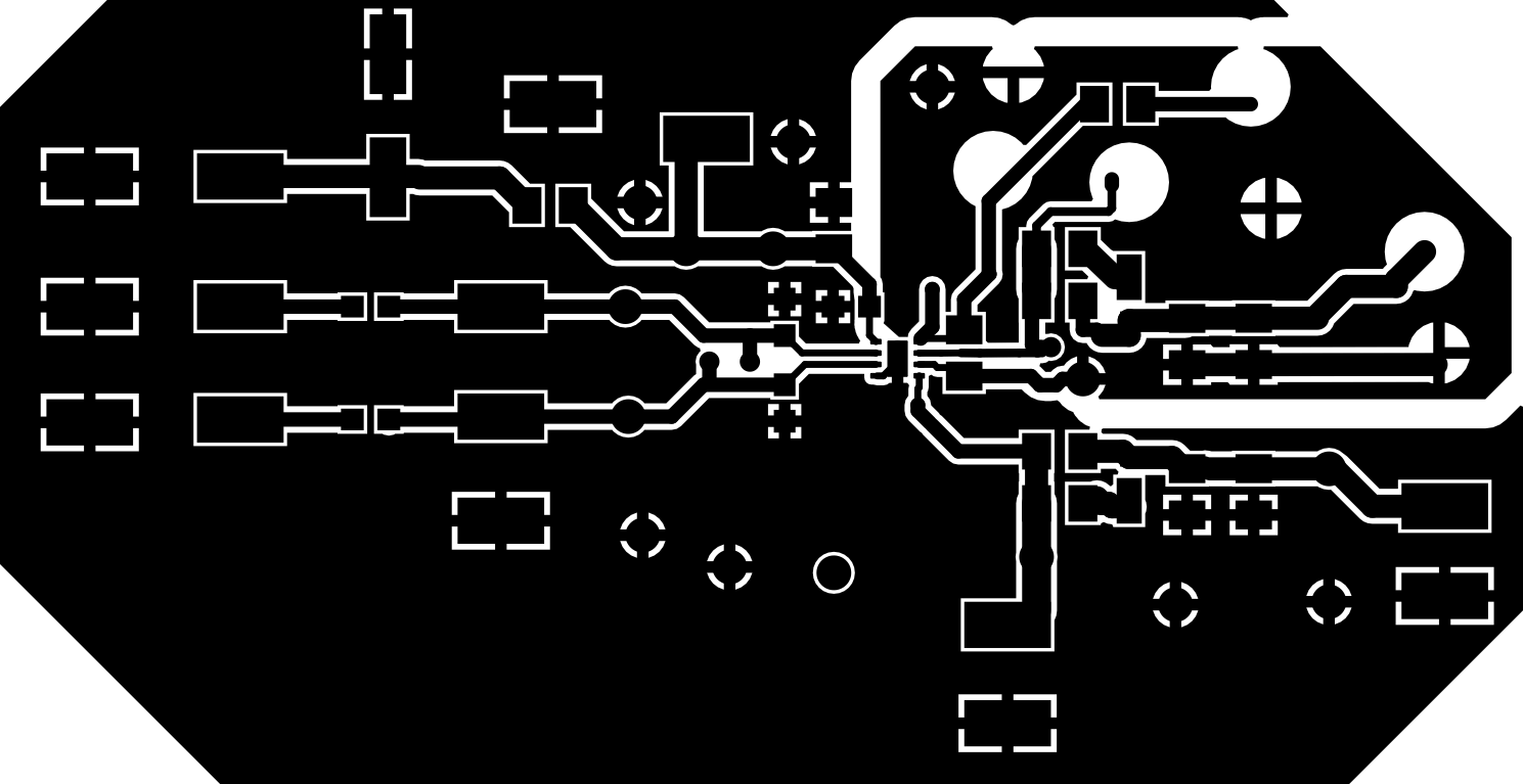
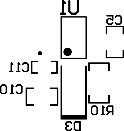
The PCB layout information for LM2105 is shown in #SLUUBM24900 through #SLUUBM28181.
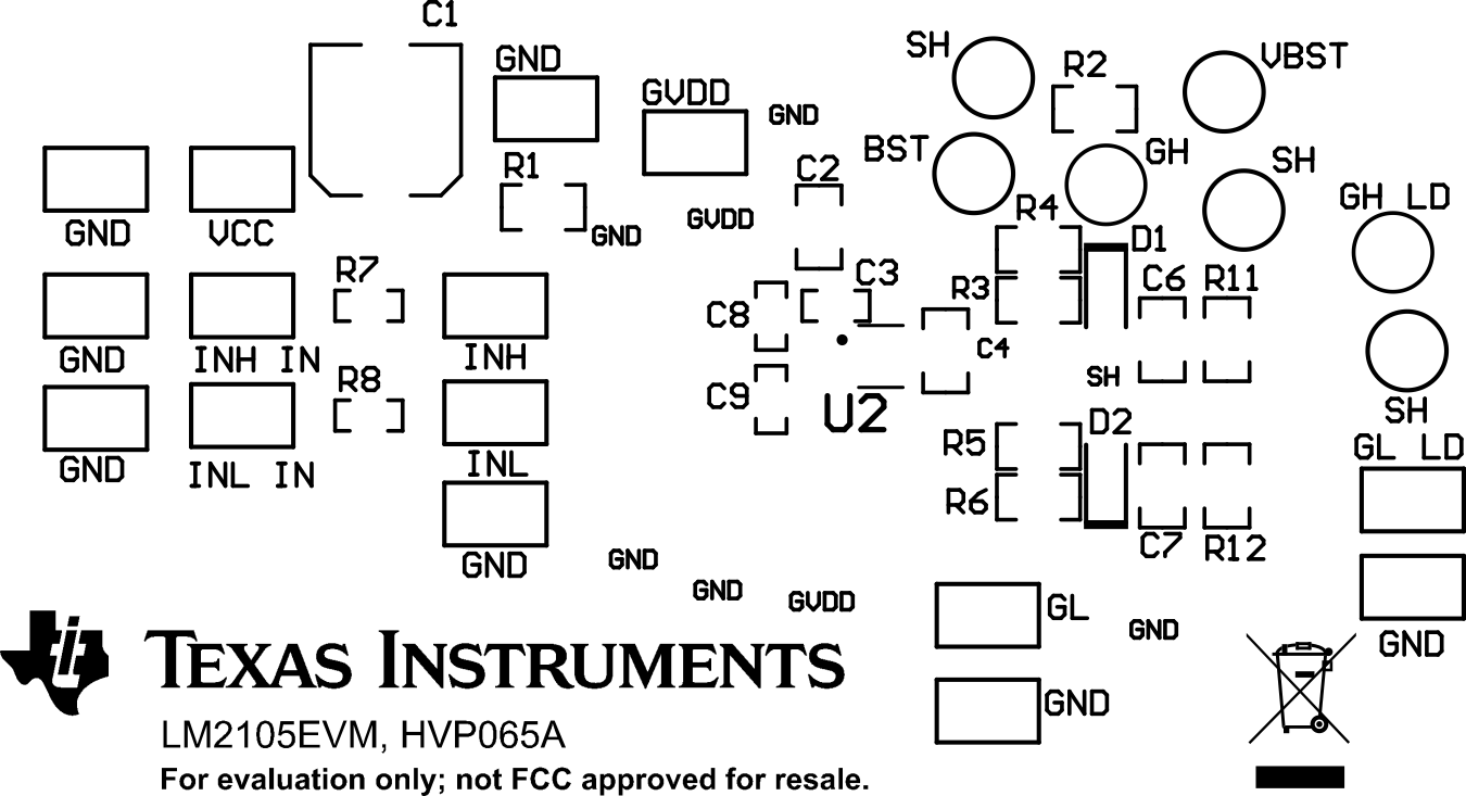
GUID-20230112-SS0I-C1QL-Z1T7-ZGW1QMX2GHFD-low.gif Figure 9-1 Top Overlay
GUID-20230112-SS0I-2XNB-XTMG-HKBKHQG2PMLJ-low.gif Figure 9-2 Top Layer
GUID-20230112-SS0I-BLJX-FCJC-FG373FV1RMRL-low.gif Figure 9-3 Bottom Layer
GUID-20230112-SS0I-4PJT-XQHL-095VFMSLHSD9-low.gif Figure 9-4 Bottom Overlay