SLVAF43 May 2021 TPS65235 , TPS65235-1 , TPS652353
3 Theoretical Analysis
Figure 3-1 shows the equivalent circuit of the typical implementation, where VLNB is the output voltage of VLNB pin and it is equivalent to a voltage source supplying to the LRC network and the load resistor Ro. Vo is the output voltage, io is the load current, isw is the current of the FET and Vsw is the voltage drop across the FET.
 Figure 3-1 Equivalent Circuit of DiSEqC™ 2.x Implementation
To reflect the attenuation of data transmission, the transfer function of Vo to VLNB is defined as follows in Equation 1
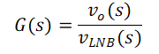
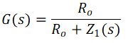
When the FET is on, assuming all component are ideal, then isw = io and Vo = VLNB. Therefore, G(s) = 1, which means there is no attenuation of the 22-kHz tone.
When the FET is off, isw = 0, the tone signal is attenuated due to LCR network. And G(s) can be expressed as Equation 2.
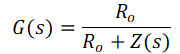
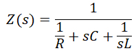
Where Z(s) can be expressed as Equation 3:
Hence the attenuation of 22-kHz tone can be expressed as Equation 4:

Figure 3-2 shows the simulation waveforms of the equivalent circuit, where GDR is the gate drive signal of the FET. It can be seen from the waveforms that there is no attenuation of the tone signal when FET is on, and when the FET is off, the attenuation of 22-kHz tone is –4.437 dB.
 Figure 3-2 Simulation Waveforms of DiSEqC™ 2.x Implementation
In practice, when the 22-kHz tone ends, VLNB is a constant voltage, but the FET will not turn off at once. So there is a constant current flowing through the FET and isw = io. After a fixed delay time tdelay, the FET turns off and isw = 0. The switching action causes a current transient ΔIsw to the FET path. At the moment the FET turns off, there will be a voltage drop across the FET due to the current transient. To better understand, the control circuit of the typical implementation can be represented by the blocks in Figure 3-3 based on Figure 3-1.
 Figure 3-3 DiSEqC™ 2.x
Implementation Control Circuit
Figure 3-3 DiSEqC™ 2.x
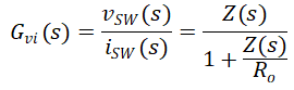
Implementation Control CircuitThe transfer function of Vsw(s) to isw(s) can be generated as Equation 5:
The inverse Laplace transform of Equation 5 allows the voltage to be expressed as Equation 6.
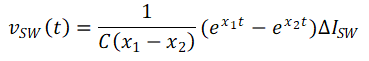
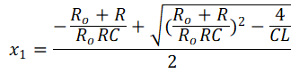
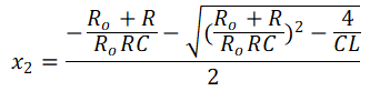
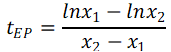
where: x1 and x2 can be expressed as Equation 7 and Equation 8.
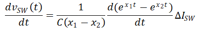
The maximum value of the voltage drop can be calculated at the extremum point tEP when the derivative of vsw(t) equals 0, and can be expressed as Equation 9:
According to Equation 9, tEP becomes Equation 10:
Considering that Ro = 22.3 Ω, so ΔIsw = 0.6 A, then Vsw_dropmax can be expressed as Equation 11:

Figure 3-4 shows the simulation results of the voltage drop across the FET, and it can be found that Vsw_dropmax = 4.59 V.
 Figure 3-4 Simulation Waveforms of Voltage Drop in DiSEqC™ 2.x Implementation
However, in practice, the voltage drop is clamped by the Vf of body diode of the FET. So the voltage drop Vsw_drop = min[Vf, Vsw_dropmax].
As previously described, adding a capacitor in series with the FET blocks the DC current path. The DC current flows continuously in the inductor and there is no transient dip when the FET is turned off. Figure 3-5 shows the equivalent circuit with the added capacitor.
 Figure 3-5 Equivalent Circuit of DiSEqC™ 2.x Implementation With
Cadd
Figure 3-5 Equivalent Circuit of DiSEqC™ 2.x Implementation With
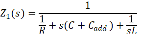
CaddThe value of the capacitor will affect the attenuation of 22-kHz tone when FET is on, and G(s) will be changed as Equation 12:
where Z1(s) can be expressed as Equation 13:
Hence the attenuation of the 22-kHz tone can expressed as Equation 14:

Based on Equation 14, Cadd can be selected to meet the maximum attenuation. For example, if the amplitude of 22-kHz tone is 650 mV, and maximum attenuation is 100 mV, then Cadd of at least 1 µF is required. Figure 3-6 shows the experimental results for 1-µF Cadd. Results for a 22-µF Cadd have already been seen in Figure 2-4.
 Figure 3-6 Experimental Results of DiSEqC™ 2.x Implementation With
Cadd
Figure 3-6 Experimental Results of DiSEqC™ 2.x Implementation With
Cadd