SLVSAB4D June   2010  – January 2017 TPS61183

PRODUCTION DATA.  

  1. Features
  2. Applications
  3. Description
  4. Revision History
  5. Pin Configuration and Functions
  6. Specifications
    1. 6.1 Absolute Maximum Ratings
    2. 6.2 ESD Ratings
    3. 6.3 Recommended Operating Conditions
    4. 6.4 Thermal Information
    5. 6.5 Electrical Characteristics
    6. 6.6 Typical Characteristics
  7. Detailed Description
    1. 7.1 Overview
    2. 7.2 Functional Block Diagram
    3. 7.3 Feature Description
      1. 7.3.1 Supply Voltage
      2. 7.3.2 Boost Regulator and Programmable Switch Frequency (FSCLT)
      3. 7.3.3 LED Current Sinks
      4. 7.3.4 Enable and Start-Up
      5. 7.3.5 IFB Pin Unused
    4. 7.4 Device Functional Modes
      1. 7.4.1 Brightness Dimming Control
      2. 7.4.2 Adjustable PWM Dimming Frequency and Mode Selection (R_FPWM/MODE)
      3. 7.4.3 Mode Selection - Programmable PWM Dimming or Direct PWM Dimming
      4. 7.4.4 Direct PWM Dimming
      5. 7.4.5 Overvoltage Clamp and Voltage Feedback (OVP/FB)
      6. 7.4.6 Current Sink Open Protection
      7. 7.4.7 Overcurrent and Short-Circuit Protection
      8. 7.4.8 Thermal Protection
      9. 7.4.9 Programmable PWM Dimming
  8. Application and Implementation
    1. 8.1 Application Information
    2. 8.2 Typical Application
      1. 8.2.1 Design Requirements
      2. 8.2.2 Detailed Design Procedure
        1. 8.2.2.1 Inductor Selection
        2. 8.2.2.2 Output Capacitor Selection
        3. 8.2.2.3 Isolation FET Selection
      3. 8.2.3 Application Curves
  9. Power Supply Recommendations
  10. 10Layout
    1. 10.1 Layout Guidelines
    2. 10.2 Layout Example
  11. 11Device and Documentation Support
    1. 11.1 Device Support
      1. 11.1.1 Third-Party Products Disclaimer
    2. 11.2 Receiving Notification of Documentation Updates
    3. 11.3 Community Resources
    4. 11.4 Trademarks
    5. 11.5 Electrostatic Discharge Caution
    6. 11.6 Glossary
  12. 12Mechanical, Packaging, and Orderable Information

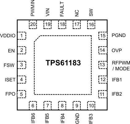
Pin Configuration and Functions

RTJ Package
20-Pin QFN With PowerPAD™
Top View
TPS61183 po_lvsab4.gif
PowerPAD™ information goes here.

Pin Functions

PIN TYPE DESCRIPTION
NO. NAME
1 VDDIO A Internal pre_regulator — connect a 1-µF ceramic capacitor to VDDIO
2 EN I Enable
3 FSW I Switching-frequency selection pin. Use a resistor to set the frequency between 280 kHz to 1 MHz.
4 ISET I Full-scale LED current set pin. Connecting a resistor to the pin programs the current level.
5 FPO O Fault protection output to indicate fault conditions including OVP, OC, and OT.
6, 7, 8,
10, 11, 12
IFB1 to IFB6 A Regulated current sink input pins
9 GND G Analog ground
13 RFPWM / MODE I Dimming frequency program pin with an external resistor / mode selection
14 OVP A Overvoltage clamp pin / voltage feedback
15 PGND G Power ground
16 SW A Drain connection of the internal power FET
17 NC No connection
18 FAULT O Fault pin to drive external ISO FET
19 VIN A Supply input pin
20 PWMIN I PWM signal input pin
PowerPAD™ Connect to GND plane for better thermal performance
A: Analog; G: Ground; I: Input: O: Output; P: Power