SLVSB70C October   2013  – January 2021 TPS62085 , TPS62086 , TPS62087

PRODUCTION DATA  

  1. Features
  2. Applications
  3. Description
  4. Revision History
  5. Device Options
  6. Pin Configuration and Functions
  7. Specifications
    1. 7.1 Absolute Maximum Ratings
    2. 7.2 ESD Ratings
    3. 7.3 Recommended Operating Conditions
    4. 7.4 Thermal Information
    5. 7.5 Electrical Characteristics
    6. 7.6 Typical Characteristics
  8. Detailed Description
    1. 8.1 Overview
    2. 8.2 Functional Block Diagram
    3. 8.3 Feature Description
      1. 8.3.1 Power Save Mode
      2. 8.3.2 100% Duty Cycle Low Dropout Operation
      3. 8.3.3 Soft Start
      4. 8.3.4 Switch Current Limit and Hiccup Short-Circuit Protection
      5. 8.3.5 Undervoltage Lockout
      6. 8.3.6 Thermal Shutdown
    4. 8.4 Device Functional Modes
      1. 8.4.1 Enable and Disable
      2. 8.4.2 Power Good
  9. Application and Implementation
    1. 9.1 Application Information
    2. 9.2 Typical Application
      1. 9.2.1 Design Requirements
      2. 9.2.2 Detailed Design Procedure
        1. 9.2.2.1 Custom Design With WEBENCH® Tools
        2. 9.2.2.2 Setting The Output Voltage
        3. 9.2.2.3 Output Filter Design
        4. 9.2.2.4 Inductor Selection
        5. 9.2.2.5 Capacitor Selection
      3. 9.2.3 Application Curves
  10. 10Power Supply Recommendations
  11. 11Layout
    1. 11.1 Layout Guidelines
    2. 11.2 Layout Example
    3. 11.3 Thermal Considerations
  12. 12Device and Documentation Support
    1. 12.1 Device Support
      1. 12.1.1 Development Support
        1. 12.1.1.1 Custom Design With WEBENCH® Tools
    2. 12.2 Documentation Support
      1. 12.2.1 Related Documentation
    3. 12.3 Receiving Notification of Documentation Updates
    4. 12.4 Support Resources
    5. 12.5 Trademarks
    6. 12.6 Electrostatic Discharge Caution
    7. 12.7 Glossary

Power Save Mode

As the load current decreases, the TPS62085, TPS62086, and TPS62087 enter Power Save Mode (PSM) operation. During Power Save Mode, the converter operates with reduced switching frequency and with a minimum quiescent current maintaining high efficiency. The power save mode occurs when the inductor current becomes discontinuous. Power Save Mode is based on a fixed on-time architecture, as related in Equation 1. The switching frequency over the whole load current range is also shown in Figure 7-1 for a typical application.
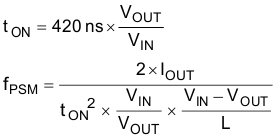
Equation 1. GUID-A2BAA592-3FCE-4ADC-921D-AA26AB8A9870-low.gif

In Power Save Mode, the output voltage rises slightly above the nominal output voltage, as shown in Figure 9-7. This effect is minimized by increasing the output capacitor or inductor value. The output voltage accuracy in PSM operation is reflected in the electrical specification table and given for a 22-μF output capacitor.

During PAUSE period in PSM (shown in Figure 8-1 ), the device does not change the PG pin state nor does it detect an UVLO event, in order to achieve a minimum quiescent current and maintain high efficiency at light loads.

GUID-4F3C2429-7E74-43E2-9892-41663DC5FCB2-low.gifFigure 8-1 Power Save Mode Waveform Diagram