SLVU097B October   2003  – October 2021 TPS54350


  1.   Trademarks
  2. 1Introduction
    1. 1.1 Background
    2. 1.2 Performance Specification Summary
    3. 1.3 Modifications
      1. 1.3.1 Output Voltage Setpoint
      2. 1.3.2 Switching Frequency
      3. 1.3.3 Input Filter
      4. 1.3.4 UVLO Programming
      5. 1.3.5 Synchronization
      6. 1.3.6 Power Good
      7. 1.3.7 Synchronous Low-Side FET
      8. 1.3.8 Optional Output Filtering
  3. 2Test Setup and Results
    1. 2.1  Input/Output Connections
    2. 2.2  Efficiency
    3. 2.3  Power Dissipation
    4. 2.4  Output Voltage Regulation
    5. 2.5  Load Transients
    6. 2.6  Loop Characteristic
    7. 2.7  Output Voltage Ripple
    8. 2.8  Input Voltage Ripple
    9. 2.9  Gate Drive
    10. 2.10 Powering Up and Down
  4. 3Board Layout
    1. 3.1 Layout
  5. 4Schematic and Bill of Materials
    1. 4.1 Bill of Materials
  6. 5Revision History

Output Voltage Regulation

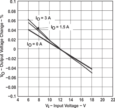
The output voltage load regulation of the TPS54350EVM−235 is shown in Figure 2-4, while the output voltage line regulation is shown in Figure 2-5. Measurements are given for an ambient temperature of 25°C.
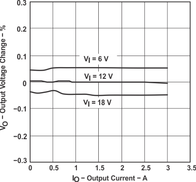
GUID-20210929-SS0I-G2G5-GJ6J-L6P5CKR1DSKK-low.gif Figure 2-4 Load Regulation
GUID-20210929-SS0I-MPTD-9Q27-B6QB5FFFJRH7-low.gif Figure 2-5 Line Regulation