SLVU097B October   2003  – October 2021 TPS54350


  1.   Trademarks
  2. 1Introduction
    1. 1.1 Background
    2. 1.2 Performance Specification Summary
    3. 1.3 Modifications
      1. 1.3.1 Output Voltage Setpoint
      2. 1.3.2 Switching Frequency
      3. 1.3.3 Input Filter
      4. 1.3.4 UVLO Programming
      5. 1.3.5 Synchronization
      6. 1.3.6 Power Good
      7. 1.3.7 Synchronous Low-Side FET
      8. 1.3.8 Optional Output Filtering
  3. 2Test Setup and Results
    1. 2.1  Input/Output Connections
    2. 2.2  Efficiency
    3. 2.3  Power Dissipation
    4. 2.4  Output Voltage Regulation
    5. 2.5  Load Transients
    6. 2.6  Loop Characteristic
    7. 2.7  Output Voltage Ripple
    8. 2.8  Input Voltage Ripple
    9. 2.9  Gate Drive
    10. 2.10 Powering Up and Down
  4. 3Board Layout
    1. 3.1 Layout
  5. 4Schematic and Bill of Materials
    1. 4.1 Bill of Materials
  6. 5Revision History

Power Dissipation

The low junction-to-case thermal resistance of the PWP package, along with a good board layout, allows the TPS54350EVM−235 EVMs to output full-rated load current while maintaining safe junction temperatures. With a 12-V input source and a load approaching the current limit of 4.2 A, the junction temperature is approximately 47°C. The total circuit losses at 25°C are shown in Figure 2-3. Power dissipation is shown for input voltages of 6 V, 12 V, and 18 V. For additional information on the dissipation ratings of the devices, see the individual product data sheets.
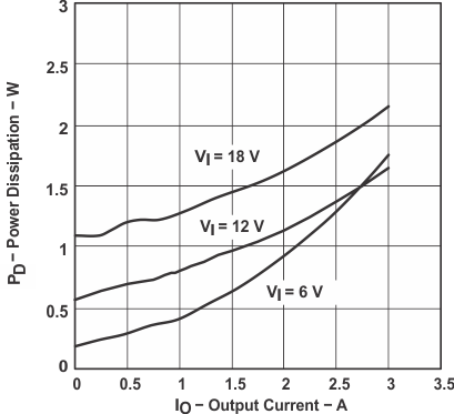
GUID-20210929-SS0I-MKVQ-ZJPK-R2KDKM6GWMWF-low.gif Figure 2-3 Measured Circuit Losses