SLYY217 September 2022 AM2631 , AM2631-Q1 , AM2632 , AM2632-Q1 , AM2634 , AM2634-Q1 , UCC14130-Q1 , UCC14131-Q1 , UCC14140-Q1 , UCC14141-Q1 , UCC14240-Q1 , UCC14241-Q1 , UCC14340-Q1 , UCC14341-Q1 , UCC15240-Q1 , UCC15241-Q1 , UCC5870-Q1 , UCC5871-Q1 , UCC5880-Q1
How gate drivers and bias supplies can support increased EV ranges
The control signals generated by the MCU and the current-sensing loop are fed to the power stage, which is the link between the battery and the motor. The power stage comprises a high-voltage DC bus decoupled by a large capacitor bank tied to three phases of power transistors, such as IGBTs or SiC MOSFETs. The power stage should have minimal power losses when translating the DC voltage to AC and be small in size in order to use the battery efficiently, which increase a vehicle’s driving range. This is a challenge, however, since components with increased voltage and power are naturally larger. Fortunately, technological breakthroughs have made it possible to keep the same component size for higher power levels.
Two factors influence traction inverter size: the type of high-voltage transistor and the voltage level of the battery. SiC MOSFETs have lower switching losses and a smaller die size when compared to IGBTs with the same voltage rating, which is why some engineers are using SiC MOSFETs in their traction inverter designs. When SiC transistors are controlled properly, they operate with fewer losses and higher reliability across all conditions in which the inverter operates, such as temperature, speed and torque, to enable increased driving ranges.
While SiC MOSFETs are more efficient, like any transistor they will experience some power loss when switching, and those switching losses can impact the efficiency of the traction inverter. The edges of voltage and current during the switching transients overlap and generate power losses, as shown in Figure 3. A high gate-driver output current results in the fast charge and discharge of the SiC FET gate to enable low power loss. It is not always the best idea to switch as fast as possible, however, given variations in switch behavior over temperature, current and voltage. The fast transitions of voltage across a SiC FET, namely the transient voltages (dv/dt) of the drain-to-source voltage (VDS), generate voltage overshoot and electromagnetic interference (EMI) in the form of conducted ground currents. The motor itself can suffer from high dv/dt given the potential for short circuits in the capacitance between the windings. Gate-driver circuitry can control both power losses and switching transients.
Using gate resistance to control the gate driver’s output source and sink current helps optimize the trade-off between dv/dt and power losses. Figure 4 shows an implementation of a gate driver with an adjustable output drive strength to optimize for changes in SiC MOSFET slew rates across temperature and current.
Adjustability is beneficial to traction inverter performance because it enables lower EMI and lower losses, resulting in higher efficiency that helps increase driving ranges. Because TI’s UCC5870-Q1 and UCC5871-Q1 gate drivers have 30-A drive strength, it is very easy to implement an adjustable gate-drive solution based on changing and optimizing the gate resistance. In addition, their galvanic isolation and 100-kV/µs CMTI enable ease of use in high-voltage applications using fast-switching SiC technologies.
The voltage level of the battery also influences the amount of dv/dt present in the system, and creates challenges when designers need to minimize EMI and choose components that can meet isolation safety standards while maintaining the same power density and area. SiC MOSFETs support high breakdown voltages >1,200 V in small die sizes, which enables a power-dense solution for 800-V EV battery applications.
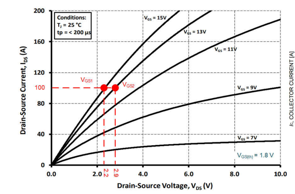
Supporting the gate voltage requirements for high-voltage SiC MOSFETs becomes challenging when the power supply needs isolation and good regulation. The impact of the gate voltage is evident from the current-voltage characteristic curve of a SiC MOSFET, shown in Figure 5, where a higher gate-to-source voltage (VGS) results in a steeper curve in its linear region. A steeper curve means a lower drain-to-source on-resistance (RDS(on)) to minimize conduction losses and avoid thermal runaway.
 Figure 5 SiC MOSFET voltage and current
characteristics based on the VGS.
Figure 5 SiC MOSFET voltage and current
characteristics based on the VGS.The isolated bias supply that provides power and voltage to the gate driver should maintain a proper positive gate voltage during fast transients and be able to support negative voltages to keep the SiC FET safely off. Transformers with semiconductor switching controllers are often used to generate isolated power supplies. Their complex design, however, directly impacts the performance of the power stage from both the electrical efficiency and EMI perspectives. The interwinding capacitance results in higher common-mode currents that lead to the generation of EMI where lower capacitance is necessary, but trade-offs between size, voltage ratings and efficiency require more time to design.
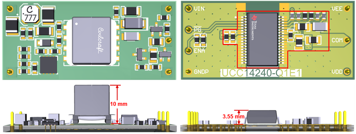
With integrated power modules such as the UCC14241-Q1 and UCC1420-Q1, the primary-to-secondary isolated capacitance can be well controlled at <3.5 pF, enabling a CMTI of >150 V/ns for fast-switching SiC MOSFETs. HEV/EV subsystem design is trending toward further integration, such as combining the traction inverter with a DC/DC converter. The UCC14241-Q1 can achieve an approximately 40% smaller bill-of-materials (BOM) area than a typical bias supply solution with a flyback converter, as shown in Figure 6. The height compared to the discrete transformer design is substantially lower, leading to a lower center of gravity and a higher vibration tolerance. All of these factors contribute to the reliability and longevity of traction inverter systems, while providing the correct voltages to efficiently drive the power transistors.
 Figure 6 BOM area and height comparison
between typical a flyback converter bias solution and the UCC14240-Q1.