SNAS407H August   2007  – April 2015 DAC128S085

PRODUCTION DATA.  

  1. Features
  2. Applications
  3. Description
  4. Revision History
  5. Description (continued)
  6. Pin Configuration and Functions
  7. Specifications
    1. 7.1 Absolute Maximum Ratings
    2. 7.2 ESD Ratings
    3. 7.3 Recommended Operating Conditions
    4. 7.4 Thermal Information
    5. 7.5 Electrical Characteristics
    6. 7.6 AC and Timing Characteristics
    7. 7.7 Typical Characteristics
  8. Detailed Description
    1. 8.1 Overview
    2. 8.2 Functional Block Diagram
    3. 8.3 Feature Description
      1. 8.3.1 DAC Architecture
      2. 8.3.2 Output Amplifiers
      3. 8.3.3 Reference Voltage
      4. 8.3.4 Serial Interface
      5. 8.3.5 Daisy-Chain Operation
      6. 8.3.6 DAC Input Data Update Mechanism
      7. 8.3.7 Power-On Reset
      8. 8.3.8 Transfer Characteristic
    4. 8.4 Device Functional Modes
      1. 8.4.1 Power-Down Modes
    5. 8.5 Programming
      1. 8.5.1 Programming the DAC128S085
        1. 8.5.1.1 Updating DAC Outputs Simultaneously
        2. 8.5.1.2 Updating DAC Outputs Independently
  9. Application and Implementation
    1. 9.1 Application Information
      1. 9.1.1 Using References as Power Supplies
    2. 9.2 Typical Application
      1. 9.2.1 Design Requirements
      2. 9.2.2 Detailed Design Procedure
      3. 9.2.3 Application Curve
  10. 10Power Supply Recommendations
  11. 11Layout
    1. 11.1 Layout Guidelines
    2. 11.2 Layout Example
  12. 12Device and Documentation Support
    1. 12.1 Device Support
      1. 12.1.1 Specification Definitions
    2. 12.2 Documentation Support
      1. 12.2.1 Related Documentation
    3. 12.3 Trademarks
    4. 12.4 Electrostatic Discharge Caution
    5. 12.5 Glossary
  13. 13Mechanical, Packaging, and Orderable Information

11 Layout

11.1 Layout Guidelines

For best accuracy and minimum noise, the printed circuit board containing the DAC128S085 should have separate analog and digital areas. The areas are defined by the locations of the analog and digital power planes. Both of these planes should be located in the same board layer. A single ground plane is preferred if digital return current does not flow through the analog ground area. Frequently a single ground plane design will utilize a "fencing" technique to prevent the mixing of analog and digital ground current. Separate ground planes should only be utilized when the fencing technique is inadequate. The separate ground planes must be connected in one place, preferably near the DAC128S085. Ensure that digital signals with fast edge rates do not pass over split ground planes. The signals must always have a continuous return path below their traces.

11.2 Layout Example
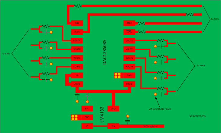
DAC128S085 Layout_SNAS407.gifFigure 34. Layout Example