SNOA985A March 2018 – February 2019 LPV821 , OPA2333 , OPA333 , TLV2333 , TLV3011 , TLV3011-Q1 , TLV3011B , TLV3011B-Q1 , TLV3012 , TLV3012-Q1 , TLV3012B , TLV3012B-Q1 , TLV333 , TLV7011 , TLV7021 , TLV7031 , TLV7041
Design Goals
| Overcurrent Levels | Supply | ||
|---|---|---|---|
| IIN (min) | IIN (max) | V+ | V– |
| –0.1 A | 1.0 A | 3.3 V | 0 V |
Design Description
This low-power, low-side, bidirectional current sensing solution uses two nano-power, zero-drift amplifiers (LPV821) and one micro-power comparator with an integrated, precision reference (TLV3012). This circuit is well-suited for battery powered devices where charging current and system current need to be monitored accurately. The gain of U1 and U2 are set independently.
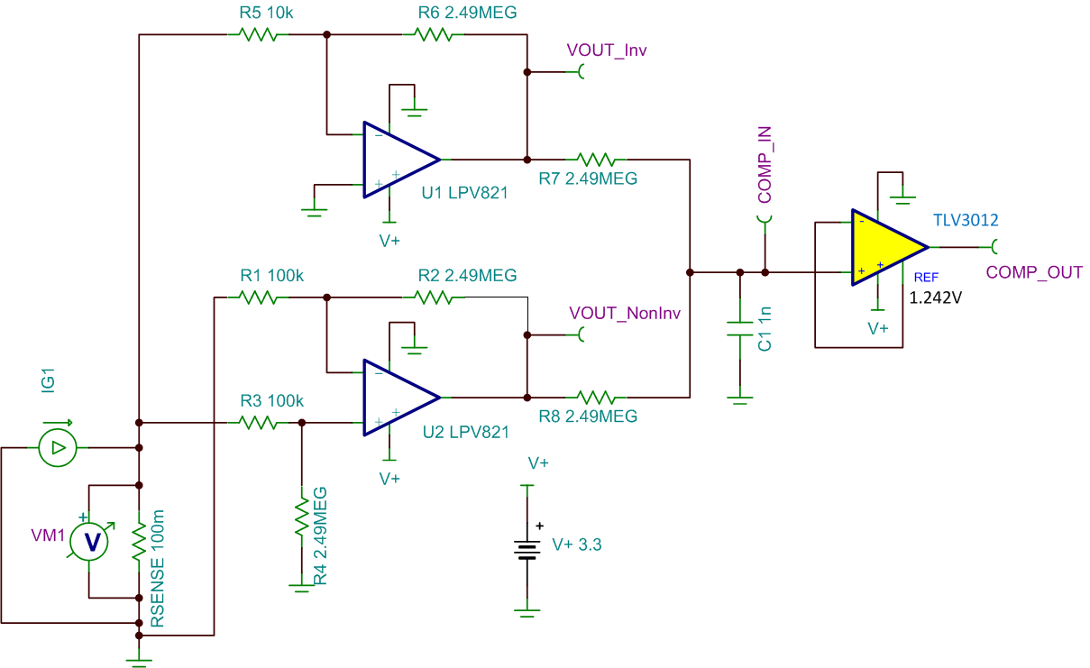
As shown in the application circuit, the LPV821 amplifiers are connected out of phase across RSENSE to amplify the currents of opposite polarity. Amplifier U2 linearly amplifies the charging (positive) current while amplifier U1 linearly amplifies the system (negative) current. When U2 is monitoring the positive current, U1 drives its output to ground. Similarly, U2 drives its ouput to ground when U1 monitors the negative current. The amplifier outputs are ORed together with resistors R7 and R8 while U1 or U2 provide the ground reference creating a single output voltage for the comparator to monitor.
If a regulated supply or reference is already available in the system, the TLV3012 can be replaced by a nano-power comparator such as the TLV7031. Moreover, if the charging current and system current have equal magnitudes, the gains of amplfier U1 and U2 can be set equal to each other. Even with the gains of the amplifiers being equal, ORing the amplifier outputs allows one comparator to detect overcurrent conditions for both charging and system current.
Design Notes
- To minimize errors, utilize precision resistors and set R1 = R3, R2 = R4, and R7 = R8 .
- Select RSENSE to minimize the voltage drop at max current and to reduce amplifier offset error when monitoring minimum current levels.
- Select the amplifier gains so COMP_IN reaches 1.242 V when the charging and system currents reach their critical levels and avoid operating the amplifiers outside of their linear range.
Design Steps
- Determine the transfer equation given R1 = R3, R2 = R4, and R7 = R8.
Inverted Path:
Non-Inverted Path:
- Select the SENSE resistor value assuming a maximum voltage drop (VSENSE) of 100 mV when charging at 1 A and a minimum system current of 10 mA.
- Select ORing resistor R7 and R8 to generate COMP_IN.
- An equal attenuation factor of two is applied to the input of the comparator with R7 =R8. Choose large values to minimize current consumption from the output of the amplifiers.
- Special care must be taken when validating the voltage at COMP_IN. Since R7 and R8 are large impedance values, the input impedance of an oscilloscope probe or the input to a digital voltmeter can alter the measured voltage. Common probe and voltmeter input impedances are 10MΩ and this will attenuate the signal measured.
- Select the amplifier gain such that COMP_IN reaches 1.242 V when the currents reach the critical threshold.
Design Simulations
DC Simulation Results (VOUT_Inv)
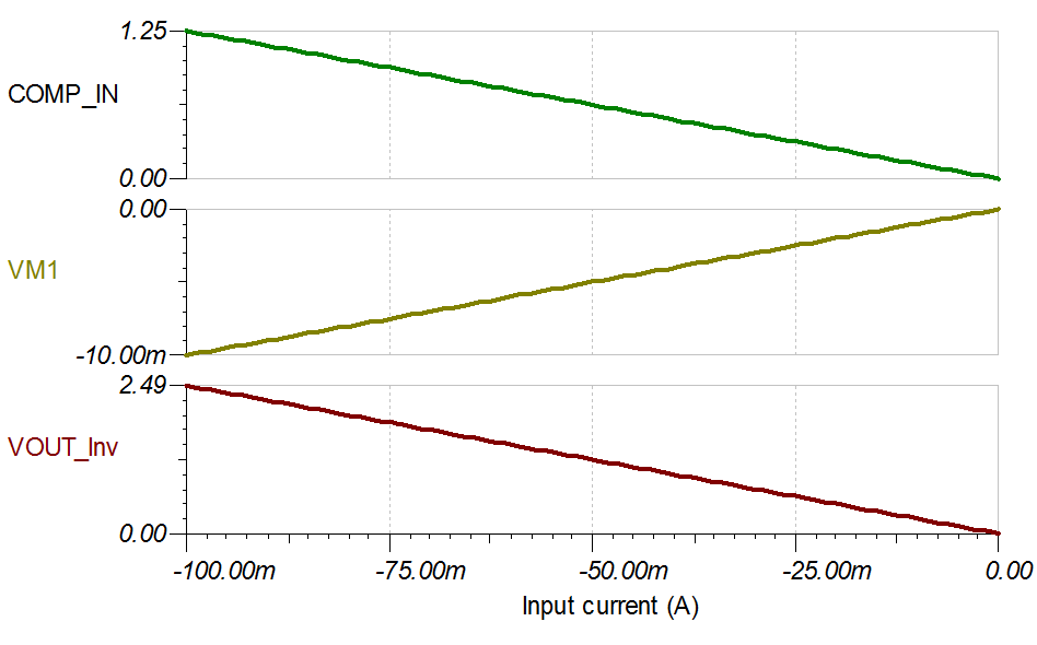
Transient Simulation Results (VOUT_Inv)
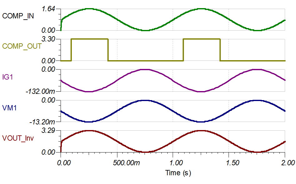
DC Simulation Results (VOUT_NonInv)
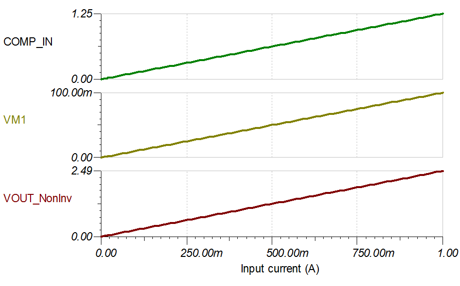
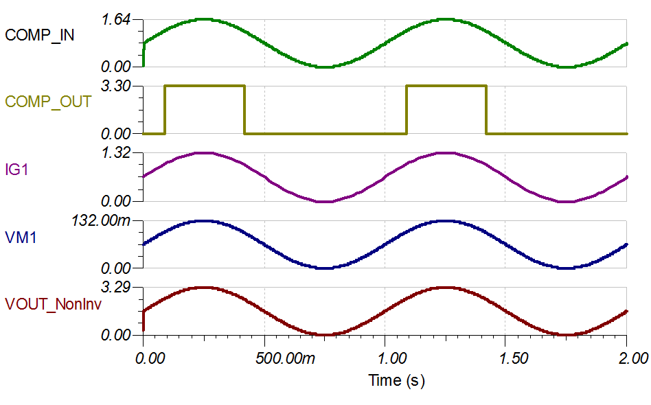
Transient Simulation Results (VOUT_NonInv)
Tech Note and Blog References
See Analog Engineer's Circuit Cookbooks for TI's comprehensive circuit library.
See Advantages of Using Nanopower Zero Drift Amp for Mobile Phone Battery Monitoring.
See Current Sensing in No-Neutral Light Switches.
See GPIO Pins Power Signal Chain in Personal Electronics Running on Li-Ion Batteries.
See Current Sensing Using NanoPower Op Amps Blog.
Design Featured Op Amp
| LPV821 | |
|---|---|
| VS | 1.7 V to 3.6 V |
| Input VCM | Rail-to-rail |
| Vout | Rail-to-rail |
| Vos | 1.5 µV |
| Vos Drift | 20 nV/°C |
| Iq | 650 nA/Ch |
| Ib | 7 pA |
| UGBW | 8 kHz |
| #Channels | 1 |
| LPV821 | |
Design Alternate Op Amp
| TLVx333 | |
|---|---|
| VS | 1.8 V to 5.5 V |
| Input VCM | Rail-to-rail |
| Vout | Rail-to-rail |
| Vos | 2 µV |
| Vos Drift | 20 nV/°C |
| Iq | 17 µA/Ch |
| Ib | 70 pA |
| UGBW | 350 kHz |
| #Channels | 1, 2, and 4 |
| TLV333 | |