SNOA999 July 2018 TLV3201 , TLV7011
Design Goals
| Supply | Input Signal | MAX AC Mains Leakage Current | |||
|---|---|---|---|---|---|
| Vcc | Vee | Type | Vi | f | Iac |
| 5 V | 0 V | Single | 240 V AC RMS | 50 Hz | <500 µA |
Design Description
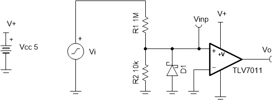
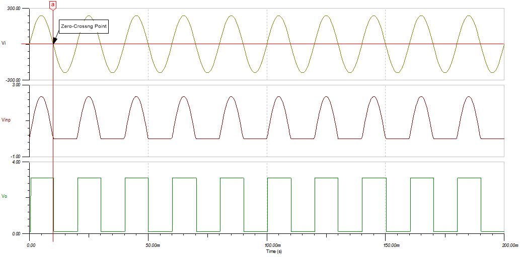
The zero crossing detector circuit changes the comparator output state when the AC input crosses the zero reference voltage. This is done by setting the comparator inverting input to the zero reference voltage and applying the attenuated input to the noninverting input.The voltage divider R1 and R2 attenuates the input AC signal. The diode D1 is used to insure the noninverting input never goes below the negative input common mode limit of the comparator. Zero crossing detection is often used in power control circuits.
Design Notes
- Some hysteresis should be used to prevent unwanted transitions due to the slow speed of the input signal.
- Select a comparator with a large input common mode range
- The phase inversion protection feature of the TLV7011 can prevent phase reversal in situations where the input goes outside of the input common mode limits
- A diode should be used to protect the comparator when the input goes below the negative input common mode limit.
Design Steps
- Calculate the peak value of the input signal.
- Select the resistor divider to attenuate the input 340 V signal down to 3.4 V in order to be within the positive common range of the comparator.
- Select R1 as 1MΩ and R2 as 10 kΩ (the closest 1% value).
- Select the diode, D1, in order to limit the negative voltage at the noninverting input. A zener diode with a voltage rating of 0.3 V can be used.
- Calculate the AC mains leakage current to check if it meets the leakage current design goal of less than 500 µA.
Design Simulations
Transient Simulation Results
Design References
See Analog Engineer's Circuit Cookbooks for TI's comprehensive circuit library.
See circuit spice simulation file, SBOMAP5.
For more information on many comparator topics including hysteresis, propagation delay and input common mode range please see, TI Precision Labs.
Design Featured Comparator
| TLV7011 | |
|---|---|
| Vss | 1.6 to 5.5V |
| VinCM | Rail-to-rail |
| tpd | 260ns |
| Vos | 0.5mV |
| VHYS | 4mV |
| Iq | 5µA |
| Output Type | Push-Pull |
| #Channels | 1 |
| TLV7011 | |
Design Alternate Comparator
| TLV3201 | |
|---|---|
| Vss | 2.7 V to 5.5 V |
| VinCM | Rail-to-rail |
| tpd | 40 ns |
| Vos | 1 V |
| VHYS | 1.2 mV |
| Iq | 40 µA |
| Output Type | Push-Pull |
| #Channels | 1 |
| TLV3201 | |