SNVAA69A October 2023 – February 2024 LM431 , LM5177 , TLV431
Introduction
The LM5177 is a synchronous buck-boost controller, which offers precise reverse current limits to charge a storage system on the input of the power stage while the output is supplied by the power supply. If there is any interruption or malfunction in the system power supply, the storage element of the power stage provides the power to the system for continuous operation. This is a single-chip design for many applications, which demand the bidirectional operation of the converter with a seamless transition between the main power supply and power backup. For instance, the design can be used in the medical domain where power-critical systems are required. Moreover, the flexibility in the scalability of the power levels enables integration with solar power systems for efficient power capturing.
The backup operation is only functional if the buck-boost controller is in FPWM mode. As a result, to enable the FPWM function, the mode pin of the controller must be high. Otherwise, the converter operates in the forward operation (PSM mode). For this operation mode the backup energy storage is connected to Vin of the LM5177 (sometimes also labeled with VBat). Once the power backup operation is enabled and the supply voltage at the output of the power stage is greater than the feedback threshold, the converter charges the storage element with a constant current at the input. The constant charging current for the storage element can be regulated using two different inbuilt current limit features of the buck-boost controller, such as peak current limit and average current limit.
To regulate the constant voltage charging for the storage element, the buck-boost controller provides various options to the customer such as, an external controller for constant voltage charging at the COMP pin and MODE pin. The purpose of this application note is to cover the constant voltage charging using external hysteresis controller at the MODE pin and the linear constant voltage controller at the COMP pin. The block diagram for the constant voltage charging using external control on the MODE pin and the COMP pin is shown in Figure 1. The subsequent sections discusses both methods for constant voltage charging.
 Figure 1 External Control for Constant Voltage Charging using MODE Pin and COMP Pin
Constant Voltage Charging using MODE Pin
The threshold voltages for the FPWM and PSM modes are 1.19V and 0.41V, respectively. If the rising edge at the MODE pin is greater than 1.19V, the converter is in FPWM mode, and the storage element charges. Similarly, if the falling edge at the MODE pin is lower than 0.41V, the converter operates in the forward direction (no backup operation), and storage discharges. The MODE pin control can be implemented in various ways, such as using a comparator with an external reference, microcontroller, and so on. These designs are expensive and require complex circuit configurations. As a result, to implement MODE pin control with a simple design, the hysteresis controller is developed using the LM431 shunt regulator, low-power PNP transistor, and low-power N-channel MOSFET. Figure 2 shows the circuit diagram for the MODE pin controller.
 Figure 2 Hysteresis Controller for MODE Pin Control
There are some important considerations for this design. Firstly, the VCC supply current for the hysteresis controller must not be more than 10mA; otherwise, the circuit overloads the VCC regulator of the buck-boost controller. The design must make sure that the minimum operating current for the LM431 (1mA). Otherwise, the device can compromise the proper functioning of the circuit. For the accurate and precise operation of the LM431 as a comparator, the cathode voltage must be higher than the reference voltage. The reference threshold voltage for the LM431 is 2.5V. The resistance combination for the voltage divider must be of higher resistance to limit the reference current of the LM431 and power losses, as the battery voltage is higher. The storage element must be precharged to fulfill the VDET condition, otherwise, the LM5177 device does not turn on.
The storage element can be of any type, such as the battery, capacitors, super-capacitors, and so on. For this application brief, the storage element is dielectric capacitors. In the design shown in Figure 2, the VCC voltage is 5V, the maximum VCC supply current is 3mA, and the constant voltage charging threshold for the storage is 30V. The constant voltage charging limit can be defined by changing the ratio of the voltage divider circuit. If the storage voltage reaches 30V, the reference voltage from the voltage divider circuit increases to 2.5V, and the cathode voltage of the LM431 decreases from VCC to 1.8V.
The decreases in the cathode voltage causes a forward biasing between the emitter-to-base terminals of the PNP transistor, and a subsequent decrease in the emitter-to-collector voltage occurs. This results in an increase in the gate-to-source voltage of the N-channel MOSFET (from 0V to VCC), and the MOSFET turns on. The MODE pin voltage decreases from VCC to 20mV. The buck-boost controller switches from FPWM mode to PSM mode, and the storage discharges. The discharging occurs until the battery voltage reaches the negative threshold of the hysteresis control. In this way, the storage voltage regulates around 30V with small hysteresis caused by the switching delay of the MOSFET.
Constant Voltage Charging using COMP Pin
The precise implementation of the inner voltage loop error amplifier reflects an accurate voltage of the COMP pin on the nominal peak current value of the inductor. Figure 3 shows the control V/I characteristics of the inner voltage loop error amplifier in FPWM mode. The value for V(comp, CL+) and V(comp, CL-) are 1.25V and 0.24V, respectively. Whereas the positive and negative limit for the peak current is defined by the peak current sense resistor.
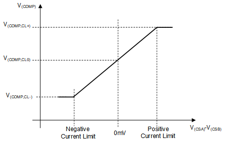 Figure 3 Control Function for the Peak Current Sense Voltage Versus VCOMP
The storage charging enables when the V(comp) value is less than the V(comp, CL0) value. Whereas the constant voltage charging of the storage activates when the V(comp) value is equal to V(comp, CL0) value. Hence, to implement the constant voltage charging using COMP pin, a closed-loop linear controller is needed. This controller charges the compensation network at the COMP pin through a current source when the storage element reaches the desired voltage level. The designed linear controller uses the TLV431 (shunt regulator) and low-power PNP transistor. The circuit diagram for the COMP pin controller is shown in Figure 4.
 Figure 4 Linear Controller for COMP Pin Control
Similar to the design of the MODE-pin controller, there are some considerations while designing the COMP-pin controller. First, the supply current for the COMP pin controller must not be more than 10mA, the design must make sure the minimum TLV431 cathode current (0.1mA), and the reference threshold voltage for the TLV431 is 1.24V. The controller design must incorporate a proper compensation network depending on the dynamics of the supply voltage. Otherwise, control loop instability issues can arise. In this design, the compensation of 100nF is added to the circuit.
The working of the COMP pin controller is similar to the MODE pin controller. The controller enables the current source at COMP pin when the biasing at the Vref pin of the TLV431 is equal to 1.24V. The constant voltage charging threshold for the linear controller is 30V. The TLV431 in the forward biasing provides appropriate PNP emitter-to-gate biasing voltages and charges the COMP pin compensation network. The reverse current of the buck-boost controller is zero, and the storage voltage remains at a constant value of 30V.
Results
To validate the precision and accuracy of the designed controllers for the MODE-pin and COMP-pin, the tests were conducted on the LM5177 Buck-Boost Controller Evaluation Module. The results in Figure 5 and Figure 6 show a smooth transition from the constant current charging to the constant voltage charging of the storage element, in the MODE pin control. The designed circuit regulates the charging voltage of the storage element around 30V. The small hysteresis caused by the switching delay of the MOSFET can be seen in the transitions between the fPWM and PSM modes during the regulation at the MODE-pin. This causes a small ripple in the charging voltage of the storage. Moreover, an initial biasing of 7.5V was given to the storage to overcome the internal low voltage protection of the buck-boost controller. The charging current during the constant voltage charging phase is limited to 2.5A by the average current limit feature of the buck-boost controller. This provides additional charging protection to the storage element and control over the charging current.
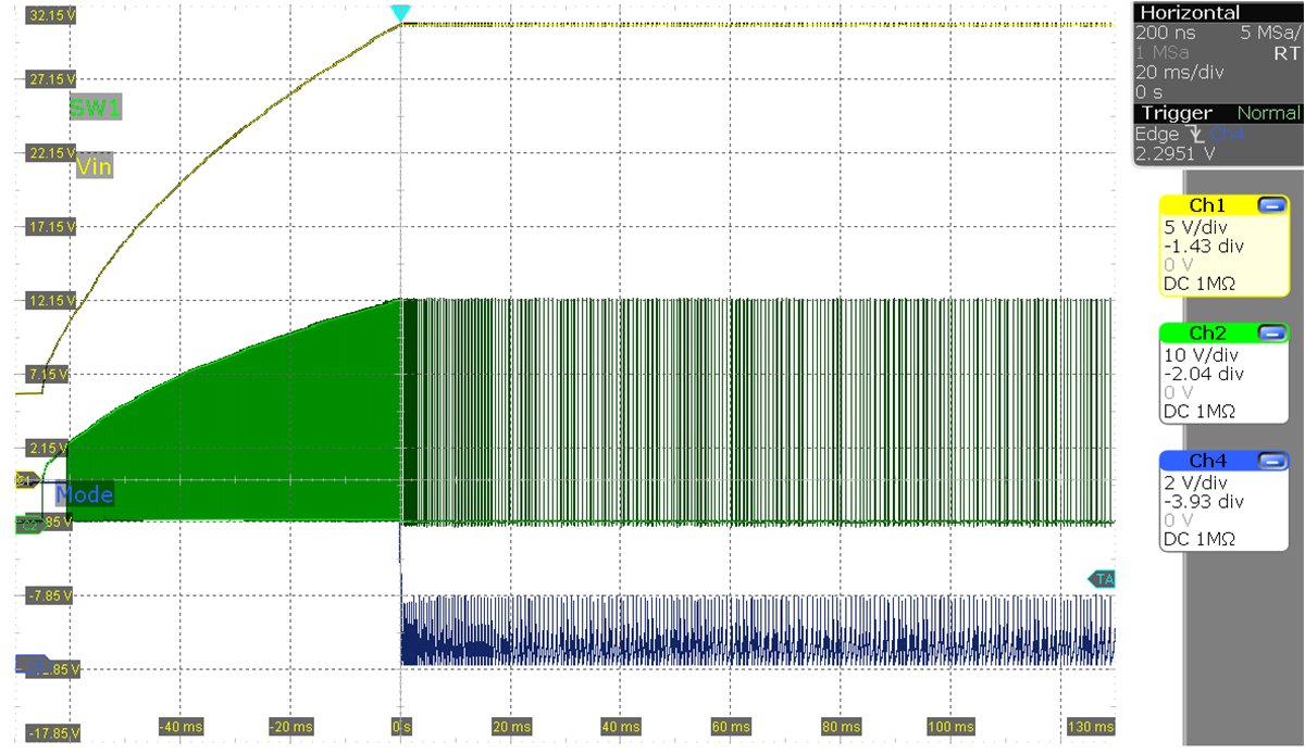 Figure 5 Scope Plot for the Constant Voltage Charging with Hysteresis Control
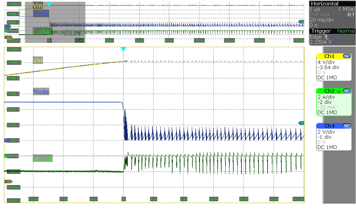 Figure 6 Zoom Plot for the Constant Voltage Charging with Hysteresis Control Zoom
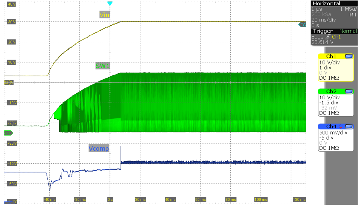 Figure 7 Plot for CV Charging with Linear Control
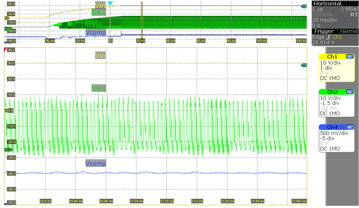 Figure 8 Plot for CV Charging with Linear Control Zoom
Figure 7 and Figure 8 shows the results for COMP-pin control. The results verify that the COMP pin control accurately regulates the storage and COMP pin voltages at 30V and 1V, respectively. Additionally, the scope plot shows a voltage spike at COMP-pin between the constant current and constant voltage transition region. To overcome this voltage spike, a higher-order compensation network, is required with the designed linear voltage controller. Moreover, the scope plot shows that the initial biasing to the storage is set to 3.4V to overcome the buck-boost controller's internal low voltage protection threshold.
Summary
The results from the above section demonstrated the seamless regulation of storage voltage during the constant voltage charging with MODE pin and COMP pin control. As a result, both constant voltage charging features are recommended for any designed application. The efficiency and supply current of the designed controllers can be improved by using a shunt regulator with a lower operating current and reference voltage, such as the TLV431 regulator used in the COMP pin controller. The hysteresis of different values can be added to the MODE pin controller by adding a small parallel current source to the voltage divider circuit or by adding a small capacitance to the MOSFET (between gate to source).
References
- Texas Instruments, LM5177 80-V Wide VIN Bidirectional 4-Switch Buck-Boost Controller, data sheet.
- Texas Instruments, Constant Current Operation Using the Internal Current Limiter, application brief.
- Texas Instruments, LM5177 Buck-Boost Controller Evaluation Module, user's guide.
- Texas Instruments, TLV431x Low-Voltage Adjustable Precision Shunt Regulator, data sheet.