SPRAAR7J November 2018 – February 2023 66AK2G12 , AM1806 , AM1808 , AM2431 , AM2432 , AM2434 , AM3351 , AM3352 , AM3354 , AM3356 , AM3357 , AM3358 , AM3358-EP , AM3359 , AM3871 , AM3874 , AM3892 , AM3894 , AM4376 , AM4377 , AM4378 , AM4379 , AM5706 , AM5708 , AM5716 , AM5718 , AM5726 , AM5728 , AM5729 , AM5746 , AM5748 , AM5749 , AM620-Q1 , AM623 , AM625 , AM625-Q1 , AM625SIP , AM62A3 , AM62A3-Q1 , AM62A7 , AM62A7-Q1 , AM62P , AM62P-Q1 , AM6411 , AM6412 , AM6421 , AM6422 , AM6441 , AM6442 , AM6526 , AM6528 , AM6546 , AM6548 , BQ24392-Q1 , HD3SS6126 , LP8727 , OMAP-L137 , OMAP5912 , TMS320C6745 , TMS320DM335 , TMS320DM355 , TMS320DM365 , TMS320DM368 , TMS320DM369 , TMS320DM6441 , TMS320DM6443 , TMS320DM6446 , TMS320DM6467 , TMS320DM8127 , TMS320DM8147 , TMS320DM8148 , TMS320DM8165 , TMS320DM8167 , TMS320DM8168 , TMS320VC5506 , TMS320VC5507 , TMS320VC5509A , TS3USB221A-Q1 , TS3USBA225 , TSU5611 , TSU6111 , TSU6111A , TSU6721 , TSU8111
- Abstract
- Trademarks
- 1Introduction
- 2General High-Speed Signal Routing
-
3High-Speed Differential Signal Routing
- 3.1 Differential Signal Spacing
- 3.2 High-Speed Differential Signal Rules
- 3.3 Symmetry in the Differential Pairs
- 3.4 Crosstalk Between the Differential Signal Pairs
- 3.5 Connectors and Receptacles
- 3.6 Via Discontinuity Mitigation
- 3.7 Back-Drill Stubs
- 3.8 Increase Via Anti-Pad Diameter
- 3.9 Equalize Via Count
- 3.10 Surface-Mount Device Pad Discontinuity Mitigation
- 3.11 Signal Bending
- 3.12 Suggested PCB Stackups
- 3.13 ESD/EMI Considerations
- 3.14 ESD/EMI Layout Rules
- 4References
- A Device Layout Parameters
- Revision History
2.1 PCB Fiber Weave Mitigation
When routing differential signals across common PCB materials, each trace of the pair will experience different dielectric constants and corresponding signal velocities due to the differences in static permittivity (Ɛr) of the fiberglass weave (Ɛr is approximately 6) and epoxy (Ɛr is approximately 3) that comprise a PCB. As signals travel faster when Ɛr is lower, an interpair skew can develop if a signal in a differential pair travels over a higher ratio of fiberglass or epoxy than does its companion signal. This skew between the differential signals can significantly degrade the differential eye diagram as presented to the receiver, cause significant AC common-mode voltage noise, and cause EMI issues. The extent of this problem will depend on the bus speed, the length of the traces, the trace geometries, the type of fiberglass weave used, and the alignment of the traces to the weave pattern of a PCB. Problems from fiber weave alignment vary from board to board. This variance makes issues difficult to diagnose.
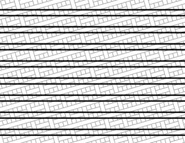
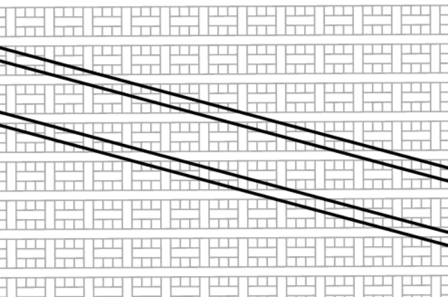
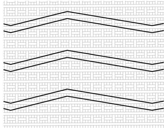
#SPRAAR72802, #SPRAAR77655, and #SPRAAR78805 show the three most common methods to minimize the impact of PCB fiber weave in a board design. The goal of each method is to ensure that both signals of the differential pair will share a relatively common Ɛr across the length of the pair routing.


Because the ratio of fiberglass to epoxy is the primary contributor to the Ɛr disparity, choose a PCB style with a tighter weave, less epoxy, and greater Ɛr uniformity across longer trace lengths. Before sending your design out for fabrication, specify a PCB style that can best accommodate high-speed signals. For examples of common PCB styles, see #SPRAAR79005.
 Figure 2-4 PCB Fiberglass Style Examples