SPRAD20 March 2022 AM2631 , AM2631-Q1 , AM2632 , AM2632-Q1 , AM2634 , AM2634-Q1
- Trademarks
- 1Introduction
-
2A Step-by-Step Guide to Running a Traction
Inverter
- 2.1 Create Real Time Debug Interface
- 2.2 Configure Control Peripheral and ADC Interrupt With Sysconfig
- 2.3 Configure Gate Driver Interface With MSPI
- 2.4 Get Samples From ADC and Read Samples Via CCS
- 2.5 Generate Space Vector PWM and Drive Motor in Open Loop
- 2.6 Close Current Loop With Mock Speed
- 2.7 Add Software Resolver to Digital Converter
- 2.8 Close Speed Loop With Rotor Speed
- 3A Brief Guide to Code Migration
- 4Summary
- 5References
2.7.1 Generate Excitation for Resolver Hardware
In Section 2.2.3, EDMA is configured to transfer data every EPWM7 SOCA event. To specify more details on the transfer, the function in the following line 1 is defined to initialize the EDMA with the location of data, size of data, and the location of DAC value register. To update the details, the function in the following line 2 is defined to change content of EDMA input table and DAC excitation output.
- uint16_t RDCexc_start(uint16_t *table, uint16_t table_size, EDMA_Handle dma_handle, uint32_t dma_ch, uint32_t dac_base)
- uint16_t RDCexc_update(uint16_t *table, uint16_t table_size, EDMA_Handle dma_handle, uint32_t dma_ch, uint32_t dac_base)
RDCexc_start should be called before control loop running, and RDCexc_update could be called while control loop running. The purpose of RDCexc_update is to reduce misalignment between excitation phase and sample time. Excitation phase can be adjusted by shifting the pointer of the input table before calling RDCexc_update. Examples are given in the following lines for both functions.
- RDCexc_start(gRDCtable_ptr,20,gEdmaHandle[0],DMA_TRIG_XBAR_EDMA_MODULE_0,CONFIG_DAC0_BASE_ADDR);
- RDCexc_update(gRDCtable_ptr,20,gEdmaHandle[0],DMA_TRIG_XBAR_EDMA_MODULE_0,CONFIG_DAC0_BASE_ADDR);
One element of a table in global scope is connected to gRDCtable_ptr. The table contains points of multiple full sine wave cycles. The element is in middle of the table so that the pointer can be shifted either right or left for excitation phase adjustment during operation. There are 20 points within one cycle. So, the length of EDMA input table is 20. EDMA handle, XBAR information and DAC address are available in configuration files.
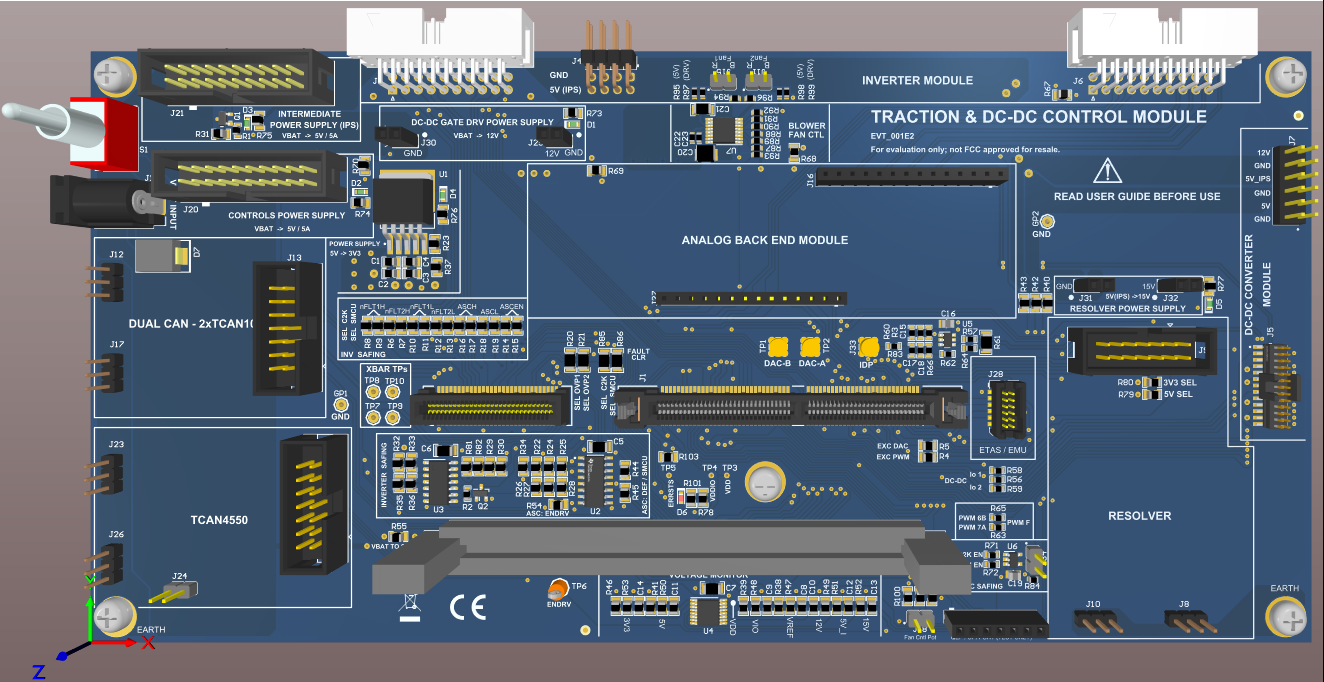
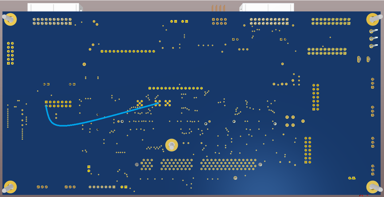
It is worth attention that there could be pin mismatches in DAC channels between TIDM-02009 mother board and some versions of AM263x control cards. The workaround is to solder a blue wire on the mother board between resolver board excitation pin and DAC-A pin. The mother board top view is given in Figure 2-42 and the connection is shown in Figure 2-43.
 Figure 2-42 Mother Board Top View
 Figure 2-43 Mother Board Blue Wire for
Resolver Excitation and DAC-A