SPRUJA7A November 2023 – April 2024
2.4 Evaluation of the Analog-to-Digital Converters (ADCs)
When using the F28P55X on-chip ADCs, there are some useful guideline to follow to realize the performance numbers listed in the device-specific data manual. This is especially true for the AC parameters such as: SNR, THD, and SINAD. Furthermore, there is a direct correlation between the SNR of the ADC result and the spread of ADC codes seen for a DC input; as such, these tips improve the range and standard deviation of a DC input as well. Finally, while topics addressed are with respect to the controlCARD, the topics are applicable to other implementations using the F28P55x MCU as well.
On-board resistors and capacitors: By default all inline resistors to the ADC pins are a simple 0Ω shunt and all capacitors to the ground plane are not populated. While this circuit can be used to supply the ADC inputs with a voltage, likely both the resistor (R) and capacitor (C) need to be populated based on the voltage source characteristics. Referring to the ADC Input Model, the ADC input has the RC network made up of the internal sample and hold capacitor, switch resistance, and parasitic capacitance. By changing the inline resistance and parallel capacitor, we can optimize the input circuit to assist with settling time and filtering the input signal. Finally, TI recommends to use Negative-Positive 0PPM/°C (NP0/C0G) capacitors as these have better stability over temperature and across input frequencies than other types of capacitors.
Voltage source and drive circuitry: While the on-chip ADCs are 12-bit architecture (4096 distinct output codes), the translation only is as precise as the input provided to the ADC. The recommended method when defining the source resolution to realize the full specification of an ADC is to have a 1-bit better source than the converter. In this case, that means that the analog input can be accurate to 13-bits.
Typically voltage supplies or regulators are not designed to be precise, but rather accommodate a wide range of current loads within a certain tolerance. For this reason, typical voltage supplies are not the best choice to show the performance of a higher bit ADC, such as the one on the F28P55x. Many times the supply in question is providing the main voltage to power the MCU; which also introduces noise and other artifacts into the signal.
In addition to the quality of the input signal, there is also the aspect of the load presented to the ADC when the ADC samples the input. An input to an ADC has zero impedance so as not to impact the internal R/C network when the sampling event takes place. In many applications, however, the voltages that are sampled by the ADC are derived from a series of resistor networks, often large in value to decrease the active current consumption of the system. A method to isolate the source impedance from the ADC sampling network is to place an operational amplifier in the signal path. Placing an operational amplifier in the signal path does not only isolate the impedance of the signal from the ADC, but also shields the source from any effects the sampling network can have on the system.
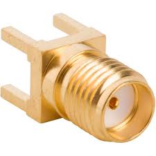
Recommended source for evaluation: The Precision Signal Injector (PSI) EVM from TI can be used to validate the ADC performance on the F28P55x ControlCARD. This EVM supports both single ended as well as differential ended outputs using a 16-bit DAC as the signal source then passed through a High Precision Op-Amp with post amplifier filtering. The EVM is powered and controlled through a standard USB connection from a host PC and includes a GUI to control the output. The outputs are routed through single or dual SMA type connectors; TI highly recommends to place an additional female SMA connector (Figure 3-3) on the controlCARD docking station to receive the signal by way of SMA for best noise immunity. For the local RC network, 30Ω resistors and 300pF capacitors were used. Using this setup, the ADC parameters were observed to be consistent with the numbers in the device-specific data sheet.
 Figure 2-3 Female SMA Connector