SSZT249 september 2020 UCC23514 , UCC5310 , UCC5320 , UCC5350 , UCC5390
You have many options when selecting an isolated gate driver for the power stage in motor-drive applications. Gate drivers can be simple or complex, with features such as an integrated Miller clamp, split outputs or an undervoltage (UVLO) lockout reference to the emitter of an insulated gate bipolar transistor (IGBT).
There are two options for input stages: a voltage input stage or current input stage. In this article, I’ll introduce both input stage options and provide a few details you should consider when selecting a gate driver with an input stage for your application.
Voltage input stage
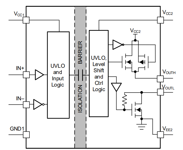
Voltage input devices accept a complementary metal-oxide semiconductor pulse-width modulation (PWM) signal directly into the gate driver on the low-voltage or primary side. Figure 1 shows an example of a typical voltage input isolated gate driver. The input pins, IN+ and IN-, are easy to drive with logic-level control signals available with most microcontrollers (MCUs). Although IN+ and IN- are on the primary side, a voltage gate driver only requires one of the inputs to receive a signal in order to function. Having both IN+ and IN- allows you to configure the PWM input signal as inverting or noninverting.
 Figure 1 Single-channel isolated gate
driver with voltage input stage
Figure 1 Single-channel isolated gate
driver with voltage input stageCurrent input stage
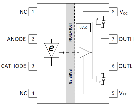
Current input devices use a current signal into the gate driver on the primary side. Figure 2 shows an example of a typical current input isolated gate driver. These devices are also referred to as optocompatible to match legacy optocouplers. In a legacy optocoupler, a current signal drives an LED inside the device to illuminate when you want the gate driver to turn on. The light emitted by the LED is received by a photodetector. The LED and photodetector are physically separated inside the optocoupler, which creates galvanic isolation from the gate driver’s primary to secondary side.
 Figure 2 Single-channel isolated gate
driver with current (optocompatible) input stage
Figure 2 Single-channel isolated gate
driver with current (optocompatible) input stageThere are system-level differences between voltage and current input gate drivers. A voltage-based solution requires fewer external components, and thus has a smaller total solution size. The MCU can drive voltage-based drivers directly, while current-based drivers need an external buffer to translate the voltage signal from the MCU into a current fed into the gate driver.
Figure 3 compares voltage input and current input gate drivers, as well as the external components required to drive an IGBT. Many designers have traditionally used current input devices to help improve noise immunity for the gate driver. Compared to a voltage signal, current signals are less susceptible to noise such as electromagnetic interference over longer distances. Adding low-pass filters to IN+ and IN- can also help increase the gate driver’s noise immunity and preserve signal integrity.
 Figure 3 Comparing voltage input and current input gate drivers
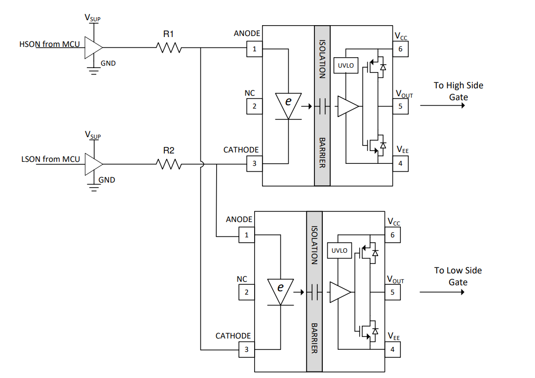
Interlock helps prevent shoot-through in motor-drive power stages, protecting the power switches in high- and low-side configurations. It is possible to achieve interlock with a current input stage gate driver by connecting the anode of the high-side driver to the cathode of the low-side driver, and vice versa. For voltage input stage gate drivers that have a single input, you can implement interlock with external logic components, or connect IN+ of the high-side driver to IN- of the low-side driver (and vice versa) if the gate driver supports both IN+ and IN-. Figure 4 shows a typical interlock example with a current input gate driver.
 Figure 4 Interlock example with current input gate driver
TI offers gate drivers for both voltage or current input options, compared below in Table 1.
| TI gate driver family | Input type | Miller clamp | Split output | Emitter-referenced UVLO | Simple single output |
|---|---|---|---|---|---|
| UCC23514 | Current | UCC23514M | UCC23514S | UCC23514E | UCC23514V |
| UCC5310 UCC5320 UCC5350 UCC5390 | Voltage | UCC5310MC, UCC5350MC | UCC5320SC, UCC5350SB, UCC5390SC | UCC5320EC, UCC5390EC | – |
A gate driver’s input stage has several implications for your motor-drive application, with system requirements dictating your selection. Whether you need to reduce the total solution size, maximize noise immunity or implement shoot-through protection, TI has many options to help you design your next motor-drive power stage.
Additional resources
- Watch the training video, “How High-Voltage Isolation Technology Works – Capacitive Structure.”
- Download the white paper, “How Capacitive Isolation Solves Key Challenges in AC Motor Drives.”
- Evaluate the UCC5320 with the UCC5320SC isolated gate driver evaluation module.