SSZTA75 may 2017 TPS65175
What does an interning doctor diagnose if he sees symptoms he has never read about in a medical handbook? A similar question can be asked of an integrated circuit (IC) validation engineer early in his career. Indeed, like a doctor, a validation engineer is assigned to evaluate the “state of health” of an IC and to make the correct “diagnosis,” which sometimes requires a deep understanding of the device “anatomy,” combined with practical experience.
A physician may begin an examination by monitoring the patient’s heartbeat. A validation engineer of a switched-mode DC/DC converter also monitors heartbeats: the switching node. But what if the switching waveform does not look like what most textbooks show? Does that indicate some kind of device “disease,” or can the engineer interpret the state as normal?
Another Waveform Audit blog "My boost converter has an off-ramp!" already explained one surprising behavior of a switching node, so in this post I will talk about “rabbit ears” – a “symptom” occurring as small bumps during switch-node toggling.
Consider a synchronous buck converter (Figure 1) operating in continuous conduction mode. At t1 (Figure 2), the low-side switch turns off and the high-side switch turns on. From t1 to t2, the high-side switch is on and Vsw is equal to VIN (neglecting RDS(on) losses). During this time, the inductor current is increasing. At t2, the high-side switch turns off, the low-side switch turns on and the inductor current starts to flow through it. From t2 to t3, the low-side switch is on, Vsw is equal to GND (neglecting RDS(on) losses). During this time, the inductor current is decreasing. At t3, the cycle starts again.
You can find typical waveform diagrams of the switching pin and inductor current shown in Figure 2 in most literature. If you go to the lab and take measurements, however, you will see that the oscilloscope picture (Figure 3) can look a bit different – it can show “rabbit ears” on the switching node at switching moments. What causes this?
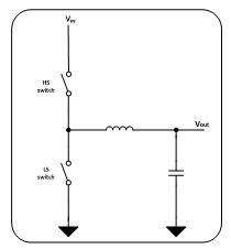 Figure 1 Simplified Diagram of a
Synchronous Buck Converter
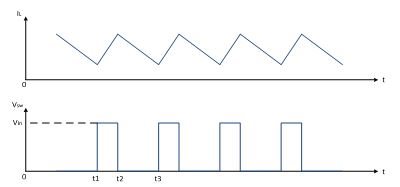 Figure 2 Waveform Diagrams of the
Inductor Current (IL) And the Switching Node (Vsw) Of a
Buck Converter Operating in Continuous Conduction Mode
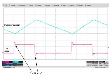 Figure 3 Oscilloscope Picture of the
Inductor Current and Switching Node with Rabbit Ears
Figure 3 Oscilloscope Picture of the
Inductor Current and Switching Node with Rabbit EarsThe secret is that the simple model shown in Figure 2 does not take into account the switching dynamics. In reality, the transition between switching phases is not instantaneous. Several nanoseconds are required to turn the transistors of the output stage on and off. To avoid cross-conduction between the switches, one should open before another starts to close. The time when both transistors are off (open) is called “dead time.”
Where does the current flow when both switches are off? In fact, metal-oxide semiconductor field-effect transistors (MOSFETs) have a parasitic body diode between the drain and the source (Figure 4), so during dead time the inductor current flows through the body diode of one of the switches. Within this time, the amplitude of the switching node increases by a value approximately equal to the diode’s forward voltage drop. This increase in amplitude shows up in the switch-node waveform as a rabbit ear.
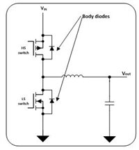 Figure 4 Simplified Diagram of the
Output Stage and Output Filter of a Synchronous Buck Converter
Figure 4 Simplified Diagram of the
Output Stage and Output Filter of a Synchronous Buck ConverterThe position of rabbit ears depends on the direction of inductor current at the moment of switching. In most applications, a buck converter sources the current. But there are applications where a buck converter should be able to sink current as well. For example, the TPS65175, a fully programmable liquid crystal display (LCD) bias IC, integrates an HVDD buck converter that can both sink and source current.
Figure 5 summarizes five cases of different positions of rabbit ears for synchronous buck converters.
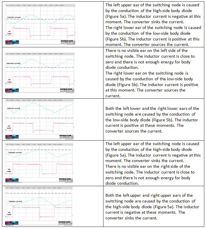 Figure 5 Different Positions of Rabbit
Ears for the Synchronous Buck Converter Depending on the Inductor Current
Direction
 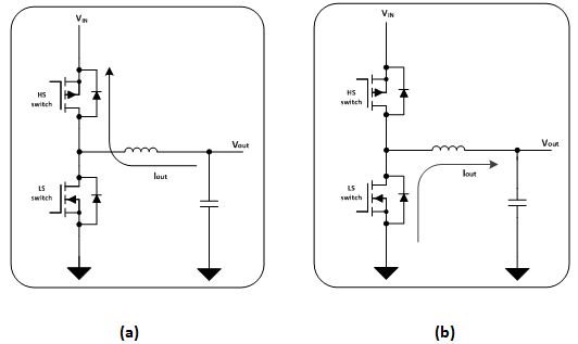 Figure 6 Conduction of the High-side
Body Diode (a); Conduction of the Low-side Body Diode (b)
Figure 6 Conduction of the High-side
Body Diode (a); Conduction of the Low-side Body Diode (b)If switching nodes were heartbeats and validation engineers were physicians, they would diagnose the presence of rabbit ears as normal. Rabbit ears do lead to a slight efficiency reduction, as some energy is lost during body diode conduction. The challenge then becomes how to optimize the switching time for switched-mode DC/DC converters.
One last thing – do not mix up rabbit ears with the ringing effect described in the Analog Applications Journal article, “Controlling switch-node ringing in synchronous buck converters,” or with the switching spikes caused by bad probe techniques.
Additional resources:
- Read the complete “Waveform audit” series: