SSZTB95 may 2016 LM20154 , LP8754 , TPS54020
Choosing the right buck-converter topology for a battery-connected automotive power supply is usually pretty straightforward. For currents up to ~3.5A, a synchronous buck converter is the best choice. A buck converter with an integrated MOSFET half bridge requires less space on the printed circuit board (PCB), fewer external components and a lower bill-of-materials cost. The synchronous design is good for efficiency and lower power dissipation, especially at higher currents.
But a buck converter is not the best choice if you need output currents higher than 3.5A because of the increasing power loss and induced rapid temperature increase. The integrated MOSFET half bridge is located on the same die as the control logic of the buck. External MOSFETs are larger and have mostly better technical characteristics, like a very low on-resistance and gate charge compared to the small integrated FETs in a buck converter.
The best choice for higher output currents is to use a buck controller with an external MOSFET half bridge to reduce the losses mentioned in the section above. Choose the MOSFETs separately from the controller so that you can scale them to your power supply’s output-power needs. The power dissipation will spread widely over the FETs and the controller, which means lower temperatures on each device. With a buck-controller topology’s flexibility, you can meet a wide range of output-power needs.
Modern applications like automotive infotainment systems are based on very powerful processors, like the Jacinto 7 from Texas Instruments. As an example, the maximum output power for the Intel Apollo Lake processor is about 40W to 50W. A power supply connected at the car battery (VIN = 3.5V to 18V, absolute maximum 42V and VOUT = 3.3V) must be able to support output currents between 8A to 12A. Most engineers would choose a buck controller to handle the high-output power requirements.
One disadvantage of a buck controller compared to a buck converter is the significantly larger current loop between the MOSFET half bridge and the external components. Larger external FETs have lower losses; the size of the package allows a better thermal connection to dissipate heat, but they are by decades larger compared to an integrated half bridge in a buck converter. The larger current loop induces parasitic effects that will result in ringing on the switch node of the power supply.
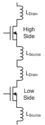
Another disadvantage of the buck-controller topology – especially when it comes to high output currents – is the fact that discrete FETs are separately packaged and have large parasitic components, like serial inductors on the drain and source. Figure 1 shows a MOSFET half-bridge equivalent circuit with parasitic inductors on the drain and source.
 Figure 1 MOSFET Half Bridge with
Parasitic Inductors LDrain and LSource
Figure 1 MOSFET Half Bridge with
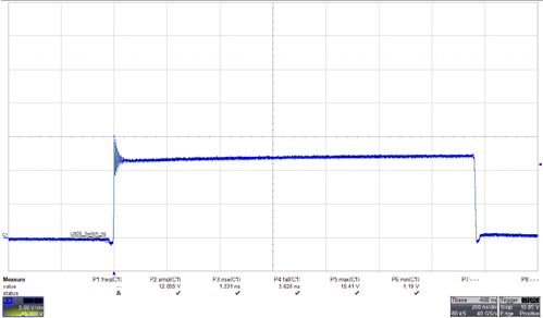
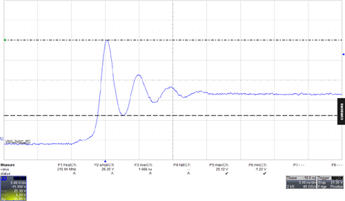
Parasitic Inductors LDrain and LSourceThe discrete FET parasitic inductors LSource and LDrain have the most significant impact on switch-node ringing and determine the ringing frequency. When the output current increases, the ringing will cause noticeable radiated electromagnetic interference (EMI). Figure 2 shows the ringing on the rising edge of the switch node of a synchronous buck controller. Figure 3 is an enlarged picture of the rising edge of the switch node. The ringing frequency is about 215MHz and is typical for a discrete packaged MOSFET.
The radiated EMI, especially in the region of about 200MHz, is unacceptable for applications like sensitive digital radio tuners (174MHz to 230MHz) or TV tuners in automotive infotainment systems.
 Figure 2 Switch Node of a Synchronous
Buck Controller. Note the Ringing on the Rising Edge. Bridge Based on a Dual
N-FET BUK9K17-60E.
 Figure 3 Close-up of the Rising Edge of
the Switch Node of a Synchronous Buck Controller with a Measured Ringing
Frequency of about 215MHz
Figure 3 Close-up of the Rising Edge of
the Switch Node of a Synchronous Buck Controller with a Measured Ringing
Frequency of about 215MHzA New Buck-converter Topology for High-output Power Requirements
So what kind of power concept should you use in an EMI-sensitive, high-power-output application? A buck converter can’t handle the output power, and a buck controller causes significant radiated EMI with increasing output currents.
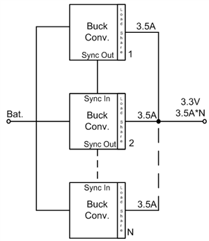
One idea is to use a single buck converter stackable to multiphase systems. The number of stacked devices depends on the maximum output current. Parasitic elements are reduced to a minimum and the power dissipation separates into multiple devices. This concept is very flexible and allows you to expand or reduce the system depending on the output current. The disadvantage is the large PCB space needed for multiple devices.
To enable this kind of topology, you will need a buck converter with an integrated load-share controller, phase synchronization – and ideally phase-shifting capability, such as the TPS54020, LM20154 and LP8754 Device Family. Figure 4 shows such a power-supply concept.
 Figure 4 A High-output-power Buck Converter Based on a Multiphase System
In conclusion, we can determine that a buck controller with external FET is not the only solution for high current power supplies in EMI-sensitive automotive infotainment systems. Using a highly integrated buck converter in a multi-phase configuration overcomes the output current limitation and provides very good EMI behavior due to the integrated MOSFET half bridge.
Additional Resources
- Learn more about TI’s buck converter topologies with these blog posts.
- Check out TI’s MOSFET portfolio.