TIDUEP0 May 2020
- Description
- Resources
- Features
- Applications
- 1Design Images
- 2System Description
-
3System Overview
- 3.1 Block Diagram
- 3.2 Design Considerations
- 3.3
Highlighted Products
- 3.3.1 TPD4E05U06 4-Channel Ultra-Low-Capacitance IEC ESD Protection Diode
- 3.3.2 TPD2EUSB30 2-Channel ESD Solution for SuperSpeed USB 3.0 Interface
- 3.3.3 2.3.3 HD3SS3220 10Gbps USB 3.1 USB Type-C 2:1 MUX With DRP Controller
- 3.3.4 TPS54218 2.95V to 6V Input, 2A Synchronous Step-Down SWIFT™ Converter
- 3.3.5 TPS54318 2.95V to 6V Input, 3A Synchronous Step-Down SWIFT™ Converter
- 3.3.6 CSD19538Q3A 100V, N ch NexFET MOSFET™, single SON3x3, 49mOhm
- 3.3.7 LM3488 2.97V to 40V Wide Vin Low-Side N-Channel Controller for Switching Regulators
- 3.3.8 TPS61178 20-V Fully Integrated Sync Boost with Load Disconnect
- 3.3.9 LMZM23601 36-V, 1-A Step-Down DC-DC Power Module in 3.8-mm × 3-mm Package
- 3.3.10 TPS7A39 Dual, 150mA, Wide-Vin, Positive and Negative Low-Dropout (LDO) Voltage Regulator
- 3.3.11 TPS74201 Single-output 1.5-A LDO regulator, adjustable (0.8V to 3.3V), any or no cap, programmable soft start
- 3.3.12 LP5910 300-mA low-noise low-IQ low-dropout (LDO) linear regulator
- 3.3.13 LP5907 250-mA ultra-low-noise low-IQ low-dropout (LDO) linear
- 3.3.14 INA231 28V, 16-bit, i2c output current/voltage/power monitor w/alert in wcsp
- 3.4
System Design Theory
- 3.4.1 Input Section
- 3.4.2
Designing of SEPIC based High Voltage Supply
- 3.4.2.1 Basic Operation Principle of SEPIC Converter
- 3.4.2.2 Design of Dual SEPIC Supply using uncoupled inductors
- 3.4.2.3 Duty Cycle
- 3.4.2.4 Inductor Selection
- 3.4.2.5 Power MOSFET Selection
- 3.4.2.6 Output Diode Selection
- 3.4.2.7 Coupling Capacitor Selection
- 3.4.2.8 Output Capacitor Selection
- 3.4.2.9 Input Capacitor Selection
- 3.4.2.10 Programming the Output Voltage
- 3.4.3 Designing the Low Voltage Power Supply
- 3.4.4 Designing the TPS54218 through Webench Power Designer
- 3.4.5 ± 5V Transmit Supply Generation
- 3.4.6 System Clock Synchronization
- 3.4.7 Power and data output connector
- 3.4.8 System Current and Power Monitoring
- 4Hardware, Software, Testing Requirements, and Test Results
- 5Layout Guidelines
- 6Design Files
- 7Software Files
- 8Related Documentation
- 9About the Author
3.4.2.1 Basic Operation Principle of SEPIC Converter
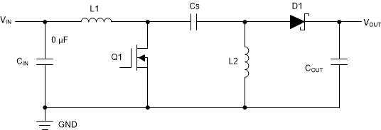
In a single ended primary inductance converter (SEPIC) design, the output voltage can be higher or lower than the input voltage. The SEPIC converter shown in Figure 9 uses two inductors: L1 and L2. The two inductors can be wound on the same core, or uncoupled since the same voltages are applied to them throughout the switching cycle.


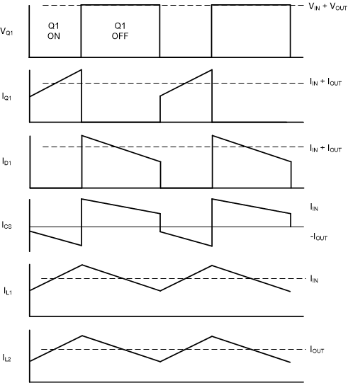
To understand the voltages at the various circuit nodes, it is important to analyze the circuit at DC when Q1 is off and not switching. During steady-state CCM, pulse-width modulation (PWM) operation, and neglecting ripple voltage, capacitor Cs is charged to the input voltage, Vin. When Q1 is off, the voltage across L2 must be Vout. Since Cin is charged to Vin, the voltage across Q1 when Q1 is off is Vin + Vout, so the voltage across L1 is Vout. When Q1 is on, capacitor C, charged to Vin, is connected in parallel with L2, so the voltage across L2 is –Vin. The currents flowing through various circuit components are shown in Figure 6. When Q1 is on, energy is being stored in L1 from the input and in L2 from Cs. When Q1 turns off, L1’s current continues to flow through Cs and D1, and into Cout and the load. Both Cout and Cs get recharged so that they can provide the load current and charge L2, respectively, when Q1 turns back on.