SNVS086K May 2000 – July 2015 LP2989LV
PRODUCTION DATA.
- 1 Features
- 2 Applications
- 3 Description
- 4 Revision History
- 5 Pin Configuration and Functions
- 6 Specifications
- 7 Detailed Description
- 8 Application and Implementation
- 9 Power Supply Recommendations
- 10Layout
- 11Device and Documentation Support
- 12Mechanical, Packaging, and Orderable Information
Package Options
Mechanical Data (Package|Pins)
- D|8
Thermal pad, mechanical data (Package|Pins)
Orderable Information
1 Features
- 2.1-V to 16-V Input Voltage Range
- Ultra-Low Dropout Voltage
- 500-mA Continuous Output Current
- Very Low Output Noise With External Capacitor
- < 0.8-µA Quiescent Current When Shut Down
- Low Ground Pin Current at All Loads
- 0.75% Output Voltage Accuracy (A Grade)
- High Peak Current Capability (800-mA typical)
- Overtemperature and Overcurrent Protection
- −40°C to +125°C Junction Temperature Range
2 Applications
- Notebooks and Desktop PCs
- PDAs and Palmtop Computers
- Wireless Communication Pins
- SMPS Post-Regulators
3 Description
The LP2989LV is a fixed-output 500-mA precision LDO regulator designed for use with ceramic output capacitors.
Output noise can be reduced to 18 μV (typical) by connecting an external 10-nF capacitor to the bypass pin.
Using an optimized Vertically Integrated PNP (VIP) process, the LP2989LV delivers superior performance:
Ground Pin Current: Typically 3 mA at 500-mA load, and 110 µA at 100-µA load.
Sleep Mode: The LP2989LV draws less than 0.8-µA quiescent current when SHUTDOWN pin is pulled low.
ERROR Flag: The built-in ERROR flag goes low when the output drops approximately 5% below nominal.
Precision Output: Output voltage accuracy is 0.75% (A grade) and 1.25% (standard grade) at room temperature.
For output voltages greater than or equal to 2 V, see the LP2989 (SNVS083) data sheet.
Device Information(1)
| PART NUMBER | PACKAGE | BODY SIZE (NOM) |
|---|---|---|
| LP2989LV | WSON (8) | 4.00 mm x 4.00 mm |
| SOIC (8) | 4.90 mm x 3.91 mm |
- For all available packages, see the orderable addendum at the end of the data sheet.
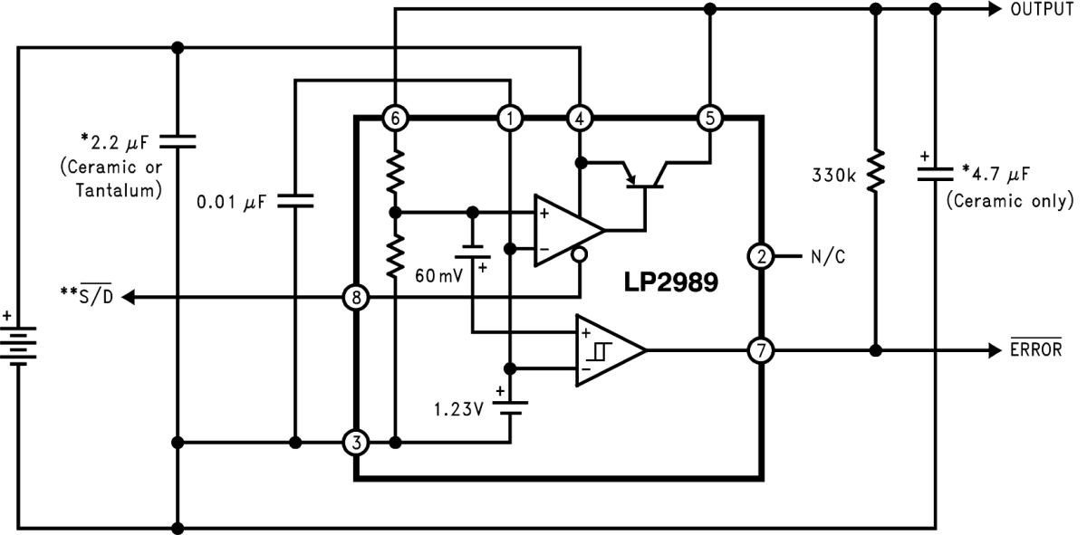
Typical Application
