SNVS673E April 2010 – September 2014 LP8551
PRODUCTION DATA.
- 1 Features
- 2 Applications
- 3 Description
- 4 Revision History
- 5 Device Default Values
- 6 Pin Configuration and Functions
-
7 Specifications
- 7.1 Absolute Maximum Ratings
- 7.2 Handling Ratings
- 7.3 Recommended Operating Conditions
- 7.4 Thermal Information
- 7.5 Electrical Characteristics
- 7.6 Boost Converter Electrical Characteristics
- 7.7 LED Driver Electrical Characteristics
- 7.8 PWM Interface Characteristics
- 7.9 Undervoltage Protection
- 7.10 Logic Interface Characteristics
- 7.11 I2C Serial Bus Timing Parameters (SDA, SCLK)
- 7.12 Typical Characteristics
-
8 Detailed Description
- 8.1 Overview
- 8.2 Functional Block Diagram
- 8.3
Feature Description
- 8.3.1 Clock Generation
- 8.3.2
Brightness Control Methods
- 8.3.2.1 PWM Input Duty Cycle
- 8.3.2.2 Brightness Register Control
- 8.3.2.3 PWM Direct Control
- 8.3.2.4 PWM Calculation Data Flow
- 8.3.2.5 PWM Detector
- 8.3.2.6 Brightness Control
- 8.3.2.7 Resolution Selector
- 8.3.2.8 Sloper
- 8.3.2.9 PWM Comparator
- 8.3.2.10 Current Setting
- 8.3.2.11 PWM Frequency Setting
- 8.3.2.12 Phase Shift PWM (PSPWM) Scheme
- 8.3.2.13 Slope
- 8.3.2.14 Driver Headroom Control
- 8.3.3 Boost Converter
- 8.3.4 Fault Detection
- 8.4 Device Functional Modes
- 8.5 Programming
- 8.6 Register Map
- 9 Application and Implementation
- 10Power Supply Recommendations
- 11Layout
- 12Device and Documentation Support
- 13Mechanical, Packaging, and Orderable Information
Package Options
Mechanical Data (Package|Pins)
- YZR|25
Thermal pad, mechanical data (Package|Pins)
Orderable Information
1 Features
- High-Voltage DC/DC Boost Converter with Integrated FET; Four Switching Frequency Options: 156/312/625/1250 kHz
- 2.7-V to 22-V Input Voltage Range to Support 1x to 5x Cell Li-Ion Batteries
- 50-mA High-Precision LED Current Sinks
- Adaptive LED Current Sink Headroom Control for Maximum System Efficiency
- Programmable PWM Resolution 8 to 13 Bits
- I2C and PWM Input Duty Cycle Brightness Control
- PWM Output Frequency and LED Current Set Through Resistors
- 4 LED Outputs with LED Fault (short/open) Detection
- Low Input Voltage, Overtemperature, Overcurrent Detection, and Shutdown
- Minimum Number of External Components
2 Applications
- Notebook and Tablet LCD Display LED Backlight
- LED Lighting
3 Description
The LP8551 is a white LED driver with integrated boost converter. It has four adjustable current sinks which can be controlled by PWM input or with I2C-compatible serial interface.
The boost converter has adaptive output voltage control based on the LED driver voltages. This feature minimizes the power consumption by adjusting the voltage to lowest sufficient level in all conditions.
LED outputs have 8-bit current resolution and up to 13-bit PWM resolution to achieve smooth and precise brightness control. Proprietary Phase Shift PWM control is used for LED outputs to reduce peak current from the boost converter, thus making the boost capacitors smaller. The Phase Shifting scheme also eliminates audible noise.
Internal EEPROM is used for storing the configuration data. This makes it possible to have minimum external component count and make the solution very small.
The LP8551 has safety features which make it possible to detect LED outputs with open or short fault. As well, low input voltage and boost overcurrent conditions are monitored, and chip is turned off in case of these events. Thermal de-rating function prevents overheating of the device by reducing backlight brightness when set temperature has been reached.
Device Information(1)
| PART NUMBER | PACKAGE | BODY SIZE (MAX) |
|---|---|---|
| LP8551 | DSBGA (25) | 2.49 mm x 2.49 mm |
- For all available packages, see the orderable addendum at the end of the datasheet.
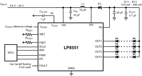
Simplified Schematic
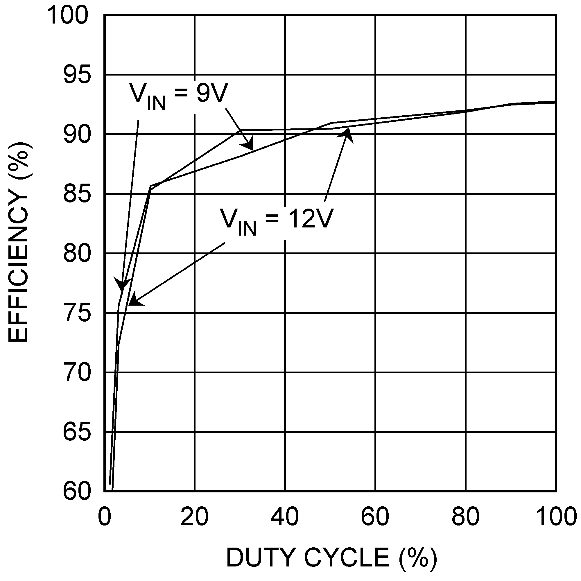
LED Drive Efficiency