SLVSC13A July 2013 – March 2016
PRODUCTION DATA.
- 1 Features
- 2 Applications
- 3 Description
- 4 Revision History
- 5 Device Comparison Table
- 6 Pin Configuration and Function
- 7 Specifications
- 8 Detailed Description
- 9 Application and Implementation
- 10Power Supply Recommendations
- 11Layout
- 12Device and Documentation Support
- 13Mechanical, Packaging, and Orderable Information
Package Options
Mechanical Data (Package|Pins)
- YFF|9
Thermal pad, mechanical data (Package|Pins)
Orderable Information
1 Features
- 2.7-V to 6.5-V Input Voltage
- Integrated 1.5-A/40-V MOSFET
- 1.2-MHz Switching Frequency
- Dual Current Sinks of up to 30-mA Current Each
- 1% Typical Current Matching and Accuracy
- 26.5-V Overvoltage Protection Threshold
- Adaptive Boost Output to WLED Voltages
- Very Low Voltage Headroom Control (90 mV)
- Flexible Digital and PWM Brightness Control
- One-Wire Control Interface (EasyScale™)
- PWM Dimming Control Interface
- Up to 100:1 PWM Dimming Ratio
- Up to 10-Bit Dimming Resolution
- Up to 90% Efficiency
- Built-in Soft Start
- Built-in WLED Open and Short Protection
- Thermal Shutdown
- Supports 4.7-µH Inductor Application
2 Applications
- Smart Phones
- PDAs, Handheld Computers
- GPS Receivers
- Backlight for Small and Media Form Factor LCD Display With Single-Cell Battery Input
3 Description
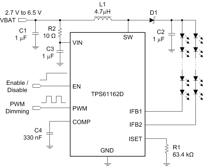
The TPS61162D is a dual-channel WLED driver which provides highly integrated solutions for single-cell Li-ion-battery-powered smart-phone backlighting. The device has a built-in high efficiency boost regulator with integrated 1.5-A/40-V power MOSFET and can support as low as 2.7-V input voltage. With two high current-matching capability current sink regulators, the device can drive up to 7s2p WLED diodes. The boost output can automatically adjust to the WLED forward voltage, allowing very low voltage headroom control, thus improving LED strings efficiency effectively.
The TPS61162D supports both the PWM dimming interface and one-wire digital EasyScale dimming interface and can realize 9-bit brightness code programming.
The TPS61162D integrates built-in soft start, overvoltage, and overcurrent protection, as well as thermal shutdown protections.
Device Information(1)
| PART NUMBER | PACKAGE | BODY SIZE (MAX) |
|---|---|---|
| TPS61162D | DSBGA (9) | 1.336 mm × 1.336 mm |
Typical Application
