SLASE51A November 2014 – November 2014 TVB1440
PRODUCTION DATA.
- 1 Features
- 2 Applications
- 3 Description
- 4 Simplified Schematics
- 5 Revision History
- 6 Pin Configuration and Functions
- 7 Specifications
- 8 Detailed Description
- 9 Application and Implementation
- 10Power Supply Recommendations
- 11Layout
- 12Device and Documentation Support
- 13Mechanical, Packaging, and Orderable Information
Package Options
Mechanical Data (Package|Pins)
- RGZ|48
Thermal pad, mechanical data (Package|Pins)
- RGZ|48
Orderable Information
1 Features
- Compatible with TV Aggregated Video Signaling Electricals
- Compatible to FPD Link 2 Interface
- Suited for Digital TV Chipset and TCON Boards
- Quad Channel Re-Driver Supporting Data Rates from 600 Mbps to 5 Gbps
- 3.3 V and 1.1 V Supply for Low Power Operation
- 175 mW Active Power Consumption for 4 Lane Operation
- 2 mW Shutdown Power
- Highly Configurable Input Equalization with 8 Control Settings
- 0 dB to 15 dB
- 4 Pre-Emphasis Control Settings
- 0, 3, 6 and 9 dB
- 4 Output Voltage Swing Control Settings
- 350, 500, 700 and 1000 mV
- I2C Control to Configure the Device for Optimum Performance
- Extended Temperature Range of -40°C to 85°C
- 2 kV HBM and 500 V CDM ESD Protection
- 48-pin QFN 7 mm x 7 mm package.
2 Applications
- Digital Television
- Camera
- Video Interfaces Requiring Large Throughputs
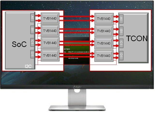
3 Description
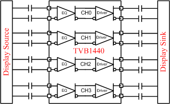
TVB1440 is a 4 channel re-driver signal conditioner for TV applications allowing signal integrity between TV chipset and TCON boards. I2C control provides the wide ranges of flexibility to configure the device for optimal signal conditioning so that video data link between a source and sink can achieve high fidelity. TVB1440 allows larger distance between a video source and sink device through its excellent jitter cleaning capability.
It has selectable control for receive equalization accessible through I2C to compensate for large trace or cable loss at its input resulting improved eye at the output signals. Transmitter in each channel has 4 levels of pre-emphasis and 4 levels of output voltage swing settings which enable optimum video signal performance from the TVB1440 to downstream receiver.
The TVB1440 is optimized for power conscience applications. Apart from its low active power, TVB1440 contains activity detection circuitry on the data link input that transitions to a low-power output disable mode in the absence of a valid input signal. This activity detect circuit can be disabled if desired. The device also has a shutdown mode when exercised results in 2mW.
Device Information(1)
| PART NUMBER | PACKAGE | BODY SIZE (NOM) |
|---|---|---|
| TVB1440 | VQFN (48) | 7.00 mm x 7.00 mm |
- For all available packages, see the orderable addendum at the end of the datasheet.
4 Simplified Schematics