DLPS074 February   2017 DLPC4422

PRODUCTION DATA.  

  1. Features
  2. Applications
  3. Description
    1.     Device Images
      1.      Simplified Schematic
  4. Revision History
  5. Pin Configuration and Functions
    1.     Pin Configurations and Functions
  6. Specifications
    1. 6.1  Absolute Maximum Ratings
    2. 6.2  ESD Ratings
    3. 6.3  Recommended Operating Conditions
    4. 6.4  Thermal Information
    5. 6.5  Electrical Characteristics
    6. 6.6  System Oscillators Timing Requirements
    7. 6.7  Test and Reset Timing Requirements
    8. 6.8  JTAG Interface: I/O Boundary Scan Application Timing Requirements
    9. 6.9  Port 1 Input Pixel Timing Requirements
    10. 6.10 Port 3 Input Pixel Interface (via GPIO) Timing Requirements
    11. 6.11 DMD LVDS Interface Timing Requirements
    12. 6.12 Synchronous Serial Port (SSP) Interface Timing Requirements
    13. 6.13 Programmable Output Clocks Switching Characteristics
    14. 6.14 Synchronous Serial Port Interface (SSP) Switching Characteristics
    15. 6.15 JTAG Interface: I/O Boundary Scan Application Switching Characteristics
  7. Detailed Description
    1. 7.1 Overview
    2. 7.2 Functional Block Diagram
    3. 7.3 Feature Description
      1. 7.3.1 System Reset Operation
        1. 7.3.1.1 Power-up Reset Operation
        2. 7.3.1.2 System Reset Operation
      2. 7.3.2 Spread Spectrum Clock Generator Support
      3. 7.3.3 GPIO Interface
      4. 7.3.4 Source Input Blanking
      5. 7.3.5 Video Graphics Processing Delay
      6. 7.3.6 Program Memory Flash/SRAM Interface
      7. 7.3.7 Calibration and Debug Support
      8. 7.3.8 Board Level Test Support
  8. Application and Implementation
    1. 8.1 Application Information
    2. 8.2 Typical Application
      1. 8.2.1 Design Requirements
        1. 8.2.1.1 Recommended MOSC Crystal Oscillator Configuration
      2. 8.2.2 Detailed Design Procedure
  9. Power Supply Recommendations
    1. 9.1 System Power Regulations
    2. 9.2 System Power-Up Sequence
    3. 9.3 Power-On Sense (POSENSE) Support
    4. 9.4 System Environment and Defaults
      1. 9.4.1 DLPC4422 System Power-Up and Reset Default Conditions
      2. 9.4.2 1.1-V System Power
      3. 9.4.3 1.8-V System Power
      4. 9.4.4 3.3-V System Power
      5. 9.4.5 Power Good (PWRGOOD) Support
      6. 9.4.6 5V Tolerant Support
  10. 10Layout
    1. 10.1 Layout Guidelines
      1. 10.1.1 PCB Layout Guidelines for Internal ASIC Power
      2. 10.1.2 PCB Layout Guidelines for Auto-Lock Performance
      3. 10.1.3 DMD Interface Considerations
      4. 10.1.4 Layout Example
      5. 10.1.5 Thermal Considerations
  11. 11Device and Documentation Support
    1. 11.1 Device Support
      1. 11.1.1 Video Timing Parameter Definitions
      2. 11.1.2 Device Nomenclature
      3. 11.1.3 Device Markings
        1. 11.1.3.1 Device Marking
    2. 11.2 Documentation Support
      1. 11.2.1 Related Documentation
    3. 11.3 Support Resources
    4. 11.4 Trademarks
    5. 11.5 Electrostatic Discharge Caution
    6. 11.6 Glossary
  12. 12Mechanical, Packaging, and Orderable Information
    1. 12.1 Package Option Addendum
      1. 12.1.1 Packaging Information

Package Options

Mechanical Data (Package|Pins)
Thermal pad, mechanical data (Package|Pins)
Orderable Information

Typical Application

The DLPC4422 controller is ideal for applications requiring high brightness and high resolution displays. When two DLPC4422 display controllers are combined with the DLP660TE DMD, an FPGA, a power management and motor driver device (DLPA100), and other electrical, optical and mechanical components the chipset enables bright, affordable, full 4K UHD display solutions. A typical 4K UHD system application using the DLPC4422 controller and DLP660TE DMD is shown in Figure 10.
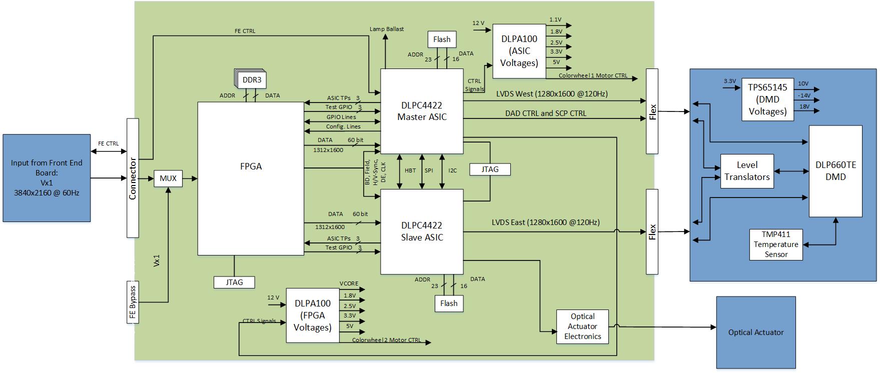
DLPC4422 TID Typical Application Block Diagram.jpgFigure 10. Typical 4K UHD Display Application