SN75LVDS32
- Meets or Exceeds the Requirements of ANSI TIA/EIA-644 Standard
- Operates With a Single 3.3-V Supply
- Designed for Signaling Rate of up to 155 Mbps
- Differential Input Thresholds ±100 mV Max
- Low-Voltage TTL (LVTTL) Logic Output Levels
- Open-Circuit Fail Safe
- Characterized For Operation From 0&dg;C to 70°C
The SN75LVDS32 and SN75LVDS9637 are differential line receivers that implement the electrical characteristics of low-voltage differential signaling (LVDS). This signaling technique lowers the output voltage levels of 5-V differential standard levels (such as EIA/TIA-422B) to reduce the power, increase the switching speeds, and allow operation with a 3.3-V supply rail. Any of the four differential receivers provides a valid logical output state with a ±100 mV allow operation with a differential input voltage within the input common-mode voltage range. The input common-mode voltage range allows 1 V of ground potential difference between two LVDS nodes.
The intended application of these devices and signaling technique is both point-to-point and multidrop (one
driver and multiple receivers) data transmission over controlled impedance media of approximately 100  . The
transmission media may be printed-circuit board traces, backplanes, or cables. The ultimate rate and distance
of data transfer is dependent upon the attenuation characteristics of the media and the noise coupling to the
environment.
. The
transmission media may be printed-circuit board traces, backplanes, or cables. The ultimate rate and distance
of data transfer is dependent upon the attenuation characteristics of the media and the noise coupling to the
environment.
The SN75LVDS32 and SN75LVDS9637 are characterized for operation from 0°C to 70°C.
技術文件
| 類型 | 標題 | 日期 | ||
|---|---|---|---|---|
| * | Data sheet | High-Speed Differential Line Receivers datasheet (Rev. B) | 2001年 6月 22日 | |
| Application brief | LVDS to Improve EMC in Motor Drives | 2018年 9月 27日 | ||
| Application brief | How Far, How Fast Can You Operate LVDS Drivers and Receivers? | 2018年 8月 3日 | ||
| Application brief | How to Terminate LVDS Connections with DC and AC Coupling | 2018年 5月 16日 | ||
| Application note | An Overview of LVDS Technology | 1998年 10月 5日 |
設計與開發
如需其他條款或必要資源,請按一下下方的任何標題以檢視詳細頁面 (如有)。
SN65LVDS31-32BEVM — 適用 LVDS31 和 LVDS32B 的 SN65LVDS31-32B 低電壓差動訊號評估模組
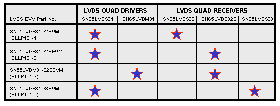
TI offers a series of low-voltage differential signaling (LVDS) evaluation modules (EVMs) designed for analysis of the electrical characteristics of LVDS drivers and receivers. Four unique EVMs are available to evaluate the different classes of LVDS devices offered by TI.
As seen (...)
SN65LVDS31-32EVM — 適用 SNx5LVDS31 和 SNx5LVDS32 的 SN65LVDS31-32EVM 評估模組
The SN65LVDS31-32EVM evaluation moduel (EVM) includes the SV65LVDS31 quad driver and the SN65LVDS32 quad receiver. The SN65LVDS31 device is a TIA/EIA-644 standard-compliant LVDS driver. The SN65LVDS32 device is a TIA/EIA-644 standard-compliant receiver that has a passive open-circuit failsafe (...)
PSPICE-FOR-TI — PSpice® for TI 設計與模擬工具
TINA-TI — 基於 SPICE 的類比模擬程式
| 封裝 | 引腳 | 下載 |
|---|---|---|
| SOIC (D) | 16 | 檢視選項 |
訂購與品質
- RoHS
- REACH
- 產品標記
- 鉛塗層/球物料
- MSL 等級/回焊峰值
- MTBF/FIT 估算值
- 材料內容
- 資格摘要
- 進行中可靠性監測
- 晶圓廠位置
- 組裝地點