SNOSBI1C November 2009 – June 2015
PRODUCTION DATA.
- 1 Features
- 2 Applications
- 3 Description
- 4 Revision History
- 5 Pin Configuration and Functions
- 6 Specifications
- 7 Parameter Measurement Information
- 8 Detailed Description
-
9 Application and Implementation
- 9.1 Application Information
- 9.2
Typical Applications
- 9.2.1
8080 Interface
- 9.2.1.1 Design Requirements
- 9.2.1.2
Detailed Design Procedure
- 9.2.1.2.1 Analog Differential Voltage Inputs and Common-Mode Rejection
- 9.2.1.2.2 Analog Inputs — Input Current
- 9.2.1.2.3 Reference Voltage
- 9.2.1.2.4 Errors and Reference Voltage Adjustments
- 9.2.1.2.5 Clocking Option
- 9.2.1.2.6 Restart During a Conversion
- 9.2.1.2.7 Continuous Conversions
- 9.2.1.2.8 Driving the Data Bus
- 9.2.1.2.9 Wiring and Hook-Up Precautions
- 9.2.2 Multiple ADC0801 Series to MC6800 CPU Interface
- 9.2.3 Auto-Zeroed Differential Transducer Amplifier and ADC Converter
- 9.2.4 Multiple ADC Converters in a Z-80 Interrupt Driven Mode
- 9.2.1
8080 Interface
- 9.3 System Examples
- 10Power Supply Recommendations
- 11Layout
- 12Device and Documentation Support
- 13Mechanical, Packaging, and Orderable Information
Package Options
Mechanical Data (Package|Pins)
- DW|20
Thermal pad, mechanical data (Package|Pins)
Orderable Information
6 Specifications
6.1 Absolute Maximum Ratings
over operating free-air temperature range (unless otherwise noted)(1)(3)| MIN | MAX | UNIT | ||
|---|---|---|---|---|
| Supply voltage (VCC)(2) | 6.5 | V | ||
| Voltage | Logic control inputs | –0.3 | 18 | V |
| At other input and outputs | –0.3 | (VCC +0.3) | ||
| Lead Temperature (Soldering, 10 seconds) | Dual-In-Line Package (plastic | 260 | °C | |
| Dual-In-Line Package (ceramic) | 300 | |||
| Surface Mount Package Vapor Phase (60 seconds) | 215 | |||
| Infrared (15 seconds) | 220 | |||
| Storage Temperature | –65 | 150 | ||
| Package Dissipation at TA = 25°C | 875 | mW | ||
(1) Stresses beyond those listed under Absolute Maximum Ratings may cause permanent damage to the device. These are stress ratings only, which do not imply functional operation of the device at these or any other conditions beyond those indicated under Recommended Operating Conditions. Exposure to absolute-maximum-rated conditions for extended periods may affect device reliability.
(2) A Zener diode exists, internally, from VCC to GND and has a typical breakdown voltage of 7 VDC.
(3) If Military/Aerospace specified devices are required, contact the Sales Office/Distributors for availability and specifications.
6.2 ESD Ratings
| VALUE | UNIT | |||
|---|---|---|---|---|
| V(ESD) | Electrostatic discharge | Human body model (HBM), per ANSI/ESDA/JEDEC JS-001(1) | ±800 | V |
(1) JEDEC document JEP155 states that 500-V HBM allows safe manufacturing with a standard ESD control process.
6.3 Recommended Operating Conditions
over operating free-air temperature range (unless otherwise noted)| MIN | NOM | MAX | UNIT | ||
|---|---|---|---|---|---|
| VCC | 4.5 | 5 | 5.5 | V | |
| Analog Input Voltage | GND – 0.05 | VCC + 0.05 | VDC | ||
6.4 Thermal Information
| THERMAL METRIC(1) | ADC080x | ADC0802, ADC0804 | UNIT | |
|---|---|---|---|---|
| NFH (PDIP) | DW (SOIC) | |||
| 20 PINS | 20 PINS | |||
| RθJA | Junction-to-ambient thermal resistance | 38.5 | 63.8 | °C/W |
| RθJC(top) | Junction-to-case (top) thermal resistance | 23.4 | 27.2 | °C/W |
| RθJB | Junction-to-board thermal resistance | 19.5 | 31.8 | °C/W |
| ψJT | Junction-to-top characterization parameter | 8.7 | 5.7 | °C/W |
| ψJB | Junction-to-board characterization parameter | 19.4 | 31.3 | °C/W |
| RθJC(bot) | Junction-to-case (bottom) thermal resistance | — | — | °C/W |
(1) For more information about traditional and new thermal metrics, see the Semiconductor and IC Package Thermal Metrics application report, SPRA953.
6.5 Operating Ratings
over operating free-air temperature range (unless otherwise noted)(1)(2).| MIN | MAX | UNIT | ||
|---|---|---|---|---|
| Temperature | ADC0804LCJ | –40 | 85 | °C |
| ADC0801/02/03/05LCN | –40 | 85 | ||
| ADC0804LCN | 0 | 70 | ||
| ADC0802/04LCWM | 0 | 70 | ||
| Range of VCC | 4.5 | 6.3 | VDC | |
(1) Absolute Maximum Ratings indicate limits beyond which damage to the device may occur. DC and AC electrical specifications do not apply when operating the device beyond its specified operating conditions.
(2) All voltages are measured with respect to GND, unless otherwise specified. The separate A GND point should always be wired to the D GND.
6.6 Electrical Characteristics
The following specifications apply for VCC = 5 VDC, TMIN ≤ TA ≤ TMAX and fCLK = 640 kHz (unless otherwise specified).| PARAMETER | TEST CONDITIONS | MIN | TYP | MAX | UNIT |
|---|---|---|---|---|---|
| ADC0801: Total Adjusted Error(1) | With Full-Scale Adj. (See Full-Scale) | ±1/4 | LSB | ||
| ADC0802: Total Unadjusted Error(1) | VREF/2=2.500 VDC | ±1/2 | |||
| ADC0803: Total Adjusted Error(1) | With Full-Scale Adj. (See Full-Scale) | ±1/2 | |||
| ADC0804: Total Unadjusted Error (1) | VREF/2=2.500 VDC | ±1 | |||
| ADC0805: Total Unadjusted Error (1) | VREF/2-No Connection | ±1 | |||
| VREF/2 Input Resistance (Pin 9) | ADC0801/02/03/05 | 2.5 | 8 | kΩ | |
| ADC0804 (2) | 0.75 | 1.1 | |||
| Analog Input Voltage Range | V(+) or V(–)(3) | GND–0.05 | VCC+0.05 | VDC | |
| DC Common-Mode Error | Over Analog Input Voltage Range | ±1/16 | ±1/8 | LSB | |
| Power Supply Sensitivity | VCC=5 VDC ±10% Over Allowed VIN(+) and VIN(–) Voltage Range(3) | ±1/16 | ±1/8 | LSB |
(1) None of these ADCs requires a zero adjust (see Zero Error). To obtain zero code at other analog input voltages see Errors and Reference Voltage Adjustments.
(2) The VREF/2 pin is the center point of a two-resistor divider connected from VCC to ground. In all versions of the ADC0801, ADC0802, ADC0803, and ADC0805, and in the ADC0804LCJ, each resistor is typically 16 kΩ. In all versions of the ADC0804 except the ADC0804LCJ, each resistor is typically 2.2 kΩ.
(3) For VIN(−)≥ VIN(+) the digital output code will be 0000 0000. Two on-chip diodes are tied to each analog input (see block diagram) which will forward conduct for analog input voltages one diode drop below ground or one diode drop greater than the VCC supply. Be careful, during testing at low VCC levels (4.5V), as high level analog inputs (5V) can cause this input diode to conduct–especially at elevated temperatures, and cause errors for analog inputs near full-scale. The spec allows 50 mV forward bias of either diode. This means that as long as the analog VIN does not exceed the supply voltage by more than 50 mV, the output code will be correct. To achieve an absolute 0 VDC to 5 VDC input voltage range will therefore require a minimum supply voltage of 4.950 VDC over temperature variations, initial tolerance and loading.
6.7 AC Electrical Characteristics
The following specifications apply for VCC=5 VDC and TMIN≤ TA≤TMAX (unless otherwise specified)| PARAMETER | TEST CONDITIONS | MIN | TYP | MAX | UNIT | ||
|---|---|---|---|---|---|---|---|
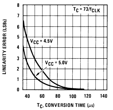
| TC | Conversion Time | fCLK = 640 kHz(1) | 103 | 114 | µs | ||
| See (2)(1) | 66 | 73 | 1/fCLK | ||||
| fCLK | Clock Frequency | VCC = 5V(2) | 100 | 640 | 1460 | kHz | |
| Clock Duty Cycle | 40% | 60% | |||||
| CR | Conversion Rate in Free-Running Mode | INTR tied to WR with CS = 0 VDC, fCLK = 640 kHz |
8770 | 9708 | conv/s | ||
| tW(WR)L | Width of WR Input (Start Pulse Width) | CS = 0 VDC (3) | 100 | ns | |||
| tACC | Access Time (Delay from Falling Edge of RD to Output Data Valid) | CL = 100 pF | 135 | 200 | |||
| t1H, t0H | Tri-State Control (Delay from Rising Edge of RD to Hi-Z State) | CL = 10 pF, RL = 10k (See Tri-State Test Circuits and Waveforms) | 125 | 200 | |||
| tWI, tRI | Delay from Falling Edge of WR or RD to Reset of INTR | 300 | 450 | ||||
| CIN | Input Capacitance of Logic Control Inputs | 5 | 7.5 | pF | |||
| COUT | Tri-State Output Capacitance (Data Buffers) | 5 | 7.5 | ||||
| CONTROL INPUTS [Note: CLK IN (Pin 4) is the input of a Schmitt trigger circuit and is therefore specified separately] | |||||||
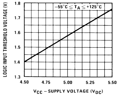
| VIN (1) | Logical “1” Input Voltage (Except Pin 4 CLK IN) | VCC = 5.25 VDC | 2 | 15 | VDC | ||
| VIN (0) | Logical “0” Input Voltage (Except Pin 4 CLK IN) | VCC = 4.75 VDC | 0.8 | ||||
| IIN (1) | Logical “1” Input Current (All Inputs) | VIN = 5 VDC | 0.005 | 1 | µADC | ||
| IIN (0) | Logical “0” Input Current (All Inputs) | VIN = 0 VDC | –1 | –0.005 | |||
| CLOCK IN AND CLOCK R | |||||||
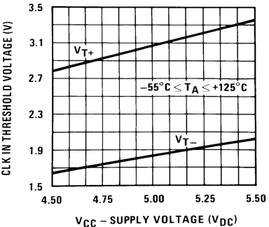
| VT+ | CLK IN (Pin 4) Positive Going Threshold Voltage | 2.7 | 3.1 | 3.5 | VDC | ||
| VT− | CLK IN (Pin 4) Negative Going Threshold Voltage | 1.5 | 1.8 | 2.1 | |||
| VH | CLK IN (Pin 4) Hysteresis (VT+)–(VT−) | 0.6 | 1.3 | 2 | |||
| VOUT (0) | Logical “0” CLK R Output Voltage | IO = 360 µA, VCC = 4.75 VDC | 0.4 | ||||
| VOUT (1) | Logical “1” CLK R Output Voltage | IO = −360 µA, VCC = 4.75 VDC | 2.4 | ||||
| DATA OUTPUTS AND INTR | |||||||
| VOUT (0) | Logical “0” Output Voltage | Data Outputs | IOUT = 1.6 mA, VCC = 4.75 VDC | 0.4 | VDC | ||
| INTR Output | IOUT = 1.0 mA, VCC = 4.75 VDC | 0.4 | |||||
| VOUT (1) | Logical “1” Output Voltage | IO = −360 µA, VCC = 4.75 VDC | 2.4 | ||||
| IO = −10 µA, VCC = 4.75 VDC | 4.5 | ||||||
| IOUT | Tri-State Disabled Output Leakage (All Data Buffers) | VOUT = 0 VDC | –3 | µADC | |||
| VOUT = 5 VDC | 3 | ||||||
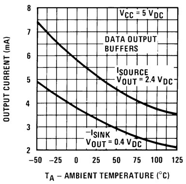
| ISOURCE | VOUT Short to GND, TA = 2 5°C | 4.5 | 6 | mADC | |||
| ISINK | VOUT Short to VCC, TA = 25°C | 9 | 16 | ||||
| POWER SUPPLY | |||||||
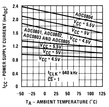
| ICC | Supply Current (Includes Ladder Current) | ADC0801/02/03/04LCJ/05 | fCLK = 640 kHz, VREF/2 = NC, TA = 25°C and CS = 5 V |
1.1 | 1.8 | mA | |
| ADC0804LCN/LCWM | 1.9 | 2.5 | |||||
(1) Accuracy is specified at fCLK = 640 kHz. At higher clock frequencies accuracy can degrade. For lower clock frequencies, the duty cycle limits can be extended so long as the minimum clock high time interval or minimum clock low time interval is no less than 275 ns.
(2) With an asynchronous start pulse, up to 8 clock periods may be required before the internal clock phases are proper to start the conversion process. The start request is internally latched. Refer to Detailed Description.
(3) The CS input is assumed to bracket the WR strobe input and therefore timing is dependent on the WR pulse width. An arbitrarily wide pulse width will hold the converter in a reset mode and the start of conversion is initiated by the low to high transition of the WR pulse.
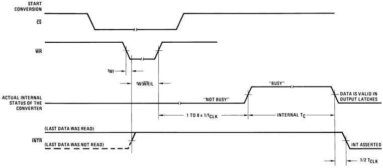 Figure 1. Start Conversion
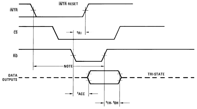
NOTE:
Read strobe must occur 8 clock periods (8/fCLK) after assertion of interrupt to specify reset of INTR.6.8 Typical Characteristics
