SLVSDR1A February   2018  – April 2020 ADC08DJ3200

PRODUCTION DATA.  

  1. Features
    1.     ADC08DJ3200 Measured Input Bandwidth
  2. Applications
  3. Description
  4. Revision History
  5. Pin Configuration and Functions
    1.     Pin Functions
  6. Specifications
    1. 6.1  Absolute Maximum Ratings
    2. 6.2  ESD Ratings
    3. 6.3  Recommended Operating Conditions
    4. 6.4  Thermal Information
    5. 6.5  Electrical Characteristics: DC Specifications
    6. 6.6  Electrical Characteristics: Power Consumption
    7. 6.7  Electrical Characteristics: AC Specifications (Dual-Channel Mode)
    8. 6.8  Electrical Characteristics: AC Specifications (Single-Channel Mode)
    9. 6.9  Timing Requirements
    10. 6.10 Switching Characteristics
    11. 6.11 Typical Characteristics
  7. Detailed Description
    1. 7.1 Overview
    2. 7.2 Functional Block Diagram
    3. 7.3 Feature Description
      1. 7.3.1 Device Comparison
      2. 7.3.2 Analog Inputs
        1. 7.3.2.1 Analog Input Protection
        2. 7.3.2.2 Full-Scale Voltage (VFS) Adjustment
        3. 7.3.2.3 Analog Input Offset Adjust
      3. 7.3.3 ADC Core
        1. 7.3.3.1 ADC Theory of Operation
        2. 7.3.3.2 ADC Core Calibration
        3. 7.3.3.3 Analog Reference Voltage
        4. 7.3.3.4 ADC Overrange Detection
        5. 7.3.3.5 Code Error Rate (CER)
      4. 7.3.4 Temperature Monitoring Diode
      5. 7.3.5 Timestamp
      6. 7.3.6 Clocking
        1. 7.3.6.1 Noiseless Aperture Delay Adjustment (tAD Adjust)
        2. 7.3.6.2 Aperture Delay Ramp Control (TAD_RAMP)
        3. 7.3.6.3 SYSREF Capture for Multi-Device Synchronization and Deterministic Latency
          1. 7.3.6.3.1 SYSREF Position Detector and Sampling Position Selection (SYSREF Windowing)
          2. 7.3.6.3.2 Automatic SYSREF Calibration
      7. 7.3.7 JESD204B Interface
        1. 7.3.7.1 Transport Layer
        2. 7.3.7.2 Scrambler
        3. 7.3.7.3 Link Layer
          1. 7.3.7.3.1 Code Group Synchronization (CGS)
          2. 7.3.7.3.2 Initial Lane Alignment Sequence (ILAS)
          3. 7.3.7.3.3 8b, 10b Encoding
          4. 7.3.7.3.4 Frame and Multiframe Monitoring
        4. 7.3.7.4 Physical Layer
          1. 7.3.7.4.1 SerDes Pre-Emphasis
        5. 7.3.7.5 JESD204B Enable
        6. 7.3.7.6 Multi-Device Synchronization and Deterministic Latency
        7. 7.3.7.7 Operation in Subclass 0 Systems
      8. 7.3.8 Alarm Monitoring
        1. 7.3.8.1 Clock Upset Detection
    4. 7.4 Device Functional Modes
      1. 7.4.1 Dual-Channel Mode
      2. 7.4.2 Single-Channel Mode (DES Mode)
      3. 7.4.3 JESD204B Modes
        1. 7.4.3.1 JESD204B Output Data Formats
      4. 7.4.4 Power-Down Modes
      5. 7.4.5 Test Modes
        1. 7.4.5.1 Serializer Test-Mode Details
        2. 7.4.5.2 PRBS Test Modes
        3. 7.4.5.3 Ramp Test Mode
        4. 7.4.5.4 Short and Long Transport Test Mode
          1. 7.4.5.4.1 Short Transport Test Pattern
        5. 7.4.5.5 D21.5 Test Mode
        6. 7.4.5.6 K28.5 Test Mode
        7. 7.4.5.7 Repeated ILA Test Mode
        8. 7.4.5.8 Modified RPAT Test Mode
      6. 7.4.6 Calibration Modes and Trimming
        1. 7.4.6.1 Foreground Calibration Mode
        2. 7.4.6.2 Background Calibration Mode
        3. 7.4.6.3 Low-Power Background Calibration (LPBG) Mode
      7. 7.4.7 Offset Calibration
      8. 7.4.8 Trimming
      9. 7.4.9 Offset Filtering
    5. 7.5 Programming
      1. 7.5.1 Using the Serial Interface
        1. 7.5.1.1 SCS
        2. 7.5.1.2 SCLK
        3. 7.5.1.3 SDI
        4. 7.5.1.4 SDO
        5. 7.5.1.5 Streaming Mode
    6. 7.6 Register Maps
      1. 7.6.1 Memory Map
      2. 7.6.2 Register Descriptions
        1. 7.6.2.1  Standard SPI-3.0 (0x000 to 0x00F)
          1. Table 23. Standard SPI-3.0 Registers
          2. 7.6.2.1.1 Configuration A Register (address = 0x000) [reset = 0x30]
            1. Table 24. CONFIG_A Field Descriptions
          3. 7.6.2.1.2 Device Configuration Register (address = 0x002) [reset = 0x00]
            1. Table 25. DEVICE_CONFIG Field Descriptions
          4. 7.6.2.1.3 Chip Type Register (address = 0x003) [reset = 0x03]
            1. Table 26. CHIP_TYPE Field Descriptions
          5. 7.6.2.1.4 Chip ID Register (address = 0x004 to 0x005) [reset = 0x0020]
            1. Table 27. CHIP_ID Field Descriptions
          6. 7.6.2.1.5 Chip Version Register (address = 0x006) [reset = 0x01]
            1. Table 28. CHIP_VERSION Field Descriptions
          7. 7.6.2.1.6 Vendor Identification Register (address = 0x00C to 0x00D) [reset = 0x0451]
            1. Table 29. VENDOR_ID Field Descriptions
        2. 7.6.2.2  User SPI Configuration (0x010 to 0x01F)
          1. 7.6.2.2.1 User SPI Configuration Register (address = 0x010) [reset = 0x00]
            1. Table 31. USR0 Field Descriptions
        3. 7.6.2.3  Miscellaneous Analog Registers (0x020 to 0x047)
          1. 7.6.2.3.1 Clock Control Register 0 (address = 0x029) [reset = 0x00]
            1. Table 33. CLK_CTRL0 Field Descriptions
          2. 7.6.2.3.2 Clock Control Register 1 (address = 0x02A) [reset = 0x00]
            1. Table 34. CLK_CTRL1 Field Descriptions
          3. 7.6.2.3.3 SYSREF Capture Position Register (address = 0x02C-0x02E) [reset = Undefined]
            1. Table 35. SYSREF_POS Field Descriptions
          4. 7.6.2.3.4 INA Full-Scale Range Adjust Register (address = 0x030-0x031) [reset = 0xA000]
            1. Table 36. FS_RANGE_A Field Descriptions
          5. 7.6.2.3.5 INB Full-Scale Range Adjust Register (address = 0x032-0x033) [reset = 0xA000]
            1. Table 37. FS_RANGE_B Field Descriptions
          6. 7.6.2.3.6 Internal Reference Bypass Register (address = 0x038) [reset = 0x00]
            1. Table 38. BG_BYPASS Field Descriptions
          7. 7.6.2.3.7 TMSTP± Control Register (address = 0x03B) [reset = 0x00]
            1. Table 39. TMSTP_CTRL Field Descriptions
        4. 7.6.2.4  Serializer Registers (0x048 to 0x05F)
          1. 7.6.2.4.1 Serializer Pre-Emphasis Control Register (address = 0x048) [reset = 0x00]
            1. Table 41. SER_PE Field Descriptions
        5. 7.6.2.5  Calibration Registers (0x060 to 0x0FF)
          1. 7.6.2.5.1  Input Mux Control Register (address = 0x060) [reset = 0x01]
            1. Table 43. INPUT_MUX Field Descriptions
          2. 7.6.2.5.2  Calibration Enable Register (address = 0x061) [reset = 0x01]
            1. Table 44. CAL_EN Field Descriptions
          3. 7.6.2.5.3  Calibration Configuration 0 Register (address = 0x062) [reset = 0x01]
            1. Table 45. CAL_CFG0 Field Descriptions
          4. 7.6.2.5.4  Calibration Status Register (address = 0x06A) [reset = Undefined]
            1. Table 46. CAL_STATUS Field Descriptions
          5. 7.6.2.5.5  Calibration Pin Configuration Register (address = 0x06B) [reset = 0x00]
            1. Table 47. CAL_PIN_CFG Field Descriptions
          6. 7.6.2.5.6  Calibration Software Trigger Register (address = 0x06C) [reset = 0x01]
            1. Table 48. CAL_SOFT_TRIG Field Descriptions
          7. 7.6.2.5.7  Low-Power Background Calibration Register (address = 0x06E) [reset = 0x88]
            1. Table 49. CAL_LP Field Descriptions
          8. 7.6.2.5.8  Calibration Data Enable Register (address = 0x070) [reset = 0x00]
            1. Table 50. CAL_DATA_EN Field Descriptions
          9. 7.6.2.5.9  Calibration Data Register (address = 0x071) [reset = Undefined]
            1. Table 51. CAL_DATA Field Descriptions
          10. 7.6.2.5.10 Channel A Gain Trim Register (address = 0x07A) [reset = Undefined]
            1. Table 52. GAIN_TRIM_A Field Descriptions
          11. 7.6.2.5.11 Channel B Gain Trim Register (address = 0x07B) [reset = Undefined]
            1. Table 53. GAIN_TRIM_B Field Descriptions
          12. 7.6.2.5.12 Band-Gap Reference Trim Register (address = 0x07C) [reset = Undefined]
            1. Table 54. BG_TRIM Field Descriptions
          13. 7.6.2.5.13 VINA Input Resistor Trim Register (address = 0x07E) [reset = Undefined]
            1. Table 55. RTRIM_A Field Descriptions
          14. 7.6.2.5.14 VINB Input Resistor Trim Register (address = 0x07F) [reset = Undefined]
            1. Table 56. RTRIM_B Field Descriptions
          15. 7.6.2.5.15 Timing Adjust for A-ADC, Single-Channel Mode, Foreground Calibration Register (address = 0x080) [reset = Undefined]
            1. Table 57. TADJ_A_FG90 Field Descriptions
          16. 7.6.2.5.16 Timing Adjust for B-ADC, Single-Channel Mode, Foreground Calibration Register (address = 0x081) [reset = Undefined]
            1. Table 58. TADJ_B_FG0 Field Descriptions
          17. 7.6.2.5.17 Timing Adjust for A-ADC, Single-Channel Mode, Background Calibration Register (address = 0x082) [reset = Undefined]
            1. Table 59. TADJ_B_FG0 Field Descriptions
          18. 7.6.2.5.18 Timing Adjust for C-ADC, Single-Channel Mode, Background Calibration Register (address = 0x083) [reset = Undefined]
            1. Table 60. TADJ_B_FG0 Field Descriptions
          19. 7.6.2.5.19 Timing Adjust for C-ADC, Single-Channel Mode, Background Calibration Register (address = 0x084) [reset = Undefined]
            1. Table 61. TADJ_B_FG0 Field Descriptions
          20. 7.6.2.5.20 Timing Adjust for B-ADC, Single-Channel Mode, Background Calibration Register (address = 0x085) [reset = Undefined]
            1. Table 62. TADJ_B_FG0 Field Descriptions
          21. 7.6.2.5.21 Timing Adjust for A-ADC, Dual-Channel Mode Register (address = 0x086) [reset = Undefined]
            1. Table 63. TADJ_A Field Descriptions
          22. 7.6.2.5.22 Timing Adjust for C-ADC Acting for A-ADC, Dual-Channel Mode Register (address = 0x087) [reset = Undefined]
            1. Table 64. TADJ_CA Field Descriptions
          23. 7.6.2.5.23 Timing Adjust for C-ADC Acting for B-ADC, Dual-Channel Mode Register (address = 0x088) [reset = Undefined]
            1. Table 65. TADJ_CB Field Descriptions
          24. 7.6.2.5.24 Timing Adjust for B-ADC, Dual-Channel Mode Register (address = 0x089) [reset = Undefined]
            1. Table 66. TADJ_B Field Descriptions
          25. 7.6.2.5.25 Offset Adjustment for A-ADC and INA Register (address = 0x08A-0x08B) [reset = Undefined]
            1. Table 67. OADJ_A_INA Field Descriptions
          26. 7.6.2.5.26 Offset Adjustment for A-ADC and INB Register (address = 0x08C-0x08D) [reset = Undefined]
            1. Table 68. OADJ_A_INB Field Descriptions
          27. 7.6.2.5.27 Offset Adjustment for C-ADC and INA Register (address = 0x08E-0x08F) [reset = Undefined]
            1. Table 69. OADJ_C_INA Field Descriptions
          28. 7.6.2.5.28 Offset Adjustment for C-ADC and INB Register (address = 0x090-0x091) [reset = Undefined]
            1. Table 70. OADJ_C_INB Field Descriptions
          29. 7.6.2.5.29 Offset Adjustment for B-ADC and INA Register (address = 0x092-0x093) [reset = Undefined]
            1. Table 71. OADJ_B_INA Field Descriptions
          30. 7.6.2.5.30 Offset Adjustment for B-ADC and INB Register (address = 0x094-0x095) [reset = Undefined]
            1. Table 72. OADJ_B_INB Field Descriptions
          31. 7.6.2.5.31 Offset Filtering Control 0 Register (address = 0x097) [reset = 0x00]
            1. Table 73. OSFILT0 Field Descriptions
          32. 7.6.2.5.32 Offset Filtering Control 1 Register (address = 0x098) [reset = 0x33]
            1. Table 74. OSFILT1 Field Descriptions
        6. 7.6.2.6  ADC Bank Registers (0x100 to 0x15F)
          1. 7.6.2.6.1  Timing Adjustment for Bank 0 (0° Clock) Register (address = 0x102) [reset = Undefined]
            1. Table 76. B0_TIME_0 Field Descriptions
          2. 7.6.2.6.2  Timing Adjustment for Bank 0 (–90° Clock) Register (address = 0x103) [reset = Undefined]
            1. Table 77. B0_TIME_90 Field Descriptions
          3. 7.6.2.6.3  Timing Adjustment for Bank 1 (0° Clock) Register (address = 0x112) [reset = Undefined]
            1. Table 78. B1_TIME_0 Field Descriptions
          4. 7.6.2.6.4  Timing Adjustment for Bank 1 (–90° Clock) Register (address = 0x113) [reset = Undefined]
            1. Table 79. B1_TIME_90 Field Descriptions
          5. 7.6.2.6.5  Timing Adjustment for Bank 2 (0° Clock) Register (address = 0x122) [reset = Undefined]
            1. Table 80. B2_TIME_0 Field Descriptions
          6. 7.6.2.6.6  Timing Adjustment for Bank 2 (–90° Clock) Register (address = 0x123) [reset = Undefined]
            1. Table 81. B2_TIME_90 Field Descriptions
          7. 7.6.2.6.7  Timing Adjustment for Bank 3 (0° Clock) Register (address = 0x132) [reset = Undefined]
            1. Table 82. B3_TIME_0 Field Descriptions
          8. 7.6.2.6.8  Timing Adjustment for Bank 3 (–90° Clock) Register (address = 0x133) [reset = Undefined]
            1. Table 83. B3_TIME_90 Field Descriptions
          9. 7.6.2.6.9  Timing Adjustment for Bank 4 (0° Clock) Register (address = 0x142) [reset = Undefined]
            1. Table 84. B4_TIME_0 Field Descriptions
          10. 7.6.2.6.10 Timing Adjustment for Bank 4 (–90° Clock) Register (address = 0x143) [reset = Undefined]
            1. Table 85. B4_TIME_90 Field Descriptions
          11. 7.6.2.6.11 Timing Adjustment for Bank 5 (0° Clock) Register (address = 0x152) [reset = Undefined]
            1. Table 86. B5_TIME_0 Field Descriptions
          12. 7.6.2.6.12 Timing Adjustment for Bank 5 (–90° Clock) Register (address = 0x153) [reset = Undefined]
            1. Table 87. B5_TIME_90 Field Descriptions
        7. 7.6.2.7  LSB Control Registers (0x160 to 0x1FF)
          1. 7.6.2.7.1 LSB Control Bit Output Register (address = 0x160) [reset = 0x00]
            1. Table 89. ENC_LSB Field Descriptions
        8. 7.6.2.8  JESD204B Registers (0x200 to 0x20F)
          1. 7.6.2.8.1  JESD204B Enable Register (address = 0x200) [reset = 0x01]
            1. Table 91. JESD_EN Field Descriptions
          2. 7.6.2.8.2  JESD204B Mode Register (address = 0x201) [reset = 0x02]
            1. Table 92. JMODE Field Descriptions
          3. 7.6.2.8.3  JESD204B K Parameter Register (address = 0x202) [reset = 0x1F]
            1. Table 93. KM1 Field Descriptions
          4. 7.6.2.8.4  JESD204B Manual SYNC Request Register (address = 0x203) [reset = 0x01]
            1. Table 94. JSYNC_N Field Descriptions
          5. 7.6.2.8.5  JESD204B Control Register (address = 0x204) [reset = 0x02]
            1. Table 95. JCTRL Field Descriptions
          6. 7.6.2.8.6  JESD204B Test Pattern Control Register (address = 0x205) [reset = 0x00]
            1. Table 96. JTEST Field Descriptions
          7. 7.6.2.8.7  JESD204B DID Parameter Register (address = 0x206) [reset = 0x00]
            1. Table 97. DID Field Descriptions
          8. 7.6.2.8.8  JESD204B Frame Character Register (address = 0x207) [reset = 0x00]
            1. Table 98. FCHAR Field Descriptions
          9. 7.6.2.8.9  JESD204B, System Status Register (address = 0x208) [reset = Undefined]
            1. Table 99. JESD_STATUS Field Descriptions
          10. 7.6.2.8.10 JESD204B Channel Power-Down Register (address = 0x209) [reset = 0x00]
            1. Table 100. PD_CH Field Descriptions
          11. 7.6.2.8.11 JESD204B Extra Lane Enable (Link A) Register (address = 0x20A) [reset = 0x00]
            1. Table 101. JESD204B Extra Lane Enable (Link A) Field Descriptions
          12. 7.6.2.8.12 JESD204B Extra Lane Enable (Link B) Register (address = 0x20B) [reset = 0x00]
            1. Table 102. JESD204B Extra Lane Enable (Link B) Field Descriptions
        9. 7.6.2.9  Digital Down Converter Registers (0x210-0x2AF)
          1. 7.6.2.9.1 Overrange Threshold 0 Register (address = 0x211) [reset = 0xF2]
            1. Table 104. OVR_T0 Field Descriptions
          2. 7.6.2.9.2 Overrange Threshold 1 Register (address = 0x212) [reset = 0xAB]
            1. Table 105. OVR_T1 Field Descriptions
          3. 7.6.2.9.3 Overrange Configuration Register (address = 0x213) [reset = 0x07]
            1. Table 106. OVR_CFG Field Descriptions
        10. 7.6.2.10 Spin Identification Register (address = 0x297) [reset = Undefined]
          1. Table 107. SPIN_ID Field Descriptions
      3. 7.6.3 SYSREF Calibration Registers (0x2B0 to 0x2BF)
        1. 7.6.3.1 SYSREF Calibration Enable Register (address = 0x2B0) [reset = 0x00]
          1. Table 109. SRC_EN Field Descriptions
        2. 7.6.3.2 SYSREF Calibration Configuration Register (address = 0x2B1) [reset = 0x05]
          1. Table 110. SRC_CFG Field Descriptions
        3. 7.6.3.3 SYSREF Calibration Status Register (address = 0x2B2 to 0x2B4) [reset = Undefined]
          1. Table 111. SRC_STATUS Field Descriptions
        4. 7.6.3.4 DEVCLK Aperture Delay Adjustment Register (address = 0x2B5 to 0x2B7) [reset = 0x000000]
          1. Table 112. TAD Field Descriptions
        5. 7.6.3.5 DEVCLK Timing Adjust Ramp Control Register (address = 0x2B8) [reset = 0x00]
          1. Table 113. TAD_RAMP Field Descriptions
      4. 7.6.4 Alarm Registers (0x2C0 to 0x2C2)
        1. 7.6.4.1 Alarm Interrupt Register (address = 0x2C0) [reset = Undefined]
          1. Table 115. ALARM Field Descriptions
        2. 7.6.4.2 Alarm Status Register (address = 0x2C1) [reset = 0x1F]
          1. Table 116. ALM_STATUS Field Descriptions
        3. 7.6.4.3 Alarm Mask Register (address = 0x2C2) [reset = 0x1F]
          1. Table 117. ALM_MASK Field Descriptions
  8. Application and Implementation
    1. 8.1 Application Information
    2. 8.2 Typical Applications
      1. 8.2.1 Wideband RF Sampling Receiver
        1. 8.2.1.1 Design Requirements
          1. 8.2.1.1.1 Input Signal Path
          2. 8.2.1.1.2 Clocking
        2. 8.2.1.2 Detailed Design Procedure
          1. 8.2.1.2.1 Calculating Values of AC-Coupling Capacitors
        3. 8.2.1.3 Application Curves
      2. 8.2.2 Reconfigurable Dual-Channel 2.5-GSPS or Single-Channel 5.0-Gsps Oscilloscope
        1. 8.2.2.1 Design Requirements
          1. 8.2.2.1.1 Input Signal Path
          2. 8.2.2.1.2 Clocking
          3. 8.2.2.1.3 ADC08DJ3200
        2. 8.2.2.2 Application Curves
    3. 8.3 Initialization Set Up
  9. Power Supply Recommendations
    1. 9.1 Power Sequencing
  10. 10Layout
    1. 10.1 Layout Guidelines
    2. 10.2 Layout Example
  11. 11Device and Documentation Support
    1. 11.1 Device Support
      1. 11.1.1 Third-Party Products Disclaimer
      2. 11.1.2 Development Support
    2. 11.2 Documentation Support
      1. 11.2.1 Related Documentation
    3. 11.3 Receiving Notification of Documentation Updates
    4. 11.4 Support Resources
    5. 11.5 Trademarks
    6. 11.6 Electrostatic Discharge Caution
    7. 11.7 Glossary
  12. 12Mechanical, Packaging, and Orderable Information

Package Options

Mechanical Data (Package|Pins)
Thermal pad, mechanical data (Package|Pins)
Orderable Information

Typical Characteristics

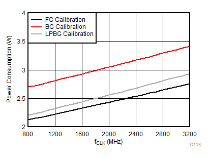
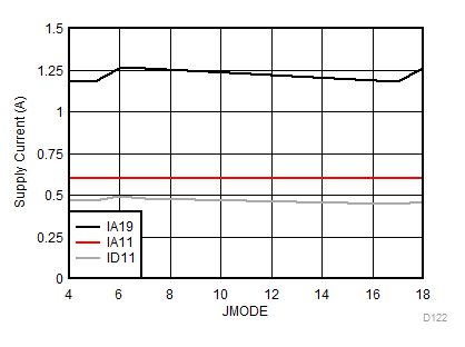
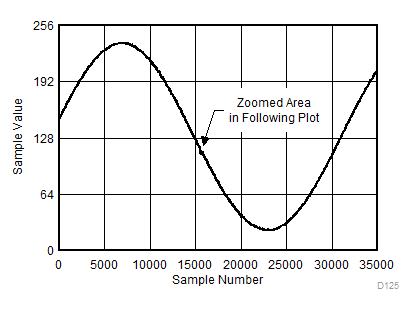
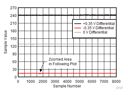
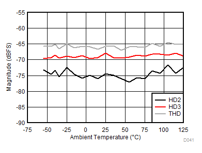
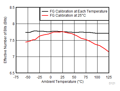
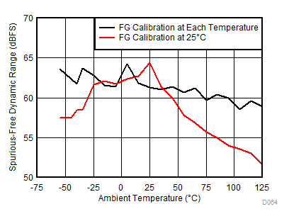
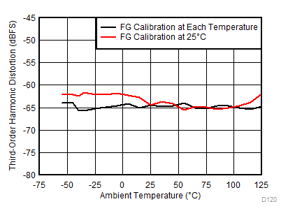
typical values at TA = 25°C, VA19 = 1.9 V, VA11 = VD11 = 1.1 V, default full-scale voltage (FS_RANGE_A = FS_RANGE_B = 0xA000), input signal applied to INA± in single-channel modes, fIN = 347 MHz, AIN = –1 dBFS, fCLK = maximum-rated clock frequency, filtered, 1-VPP sine-wave clock, JMODE = 17, and background calibration (unless otherwise noted); SNR results exclude DC, HD2 to HD9 and interleaving spurs; SINAD, ENOB, and SFDR results exclude DC and fixed-frequency interleaving spurs
ADC08DJ3200 D010_SLVSDR1.gif
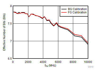
JMODE7, fS = 3200 MSPS, foreground (FG) and background (BG) calibration
Figure 4. ENOB vs Input Frequency
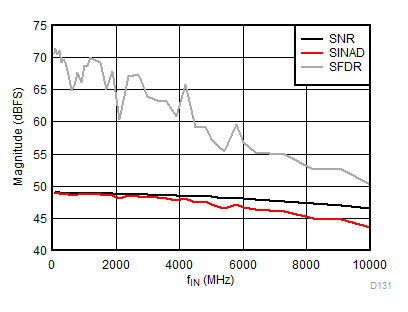
ADC08DJ3200 D131_SLVSDR1.gif
JMODE7, fS = 3200 MSPS, FG calibration
Figure 6. SNR, SINAD, SFDR vs Input Frequency
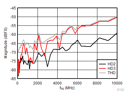
ADC08DJ3200 D132_SLVSDR1.gif
JMODE7, fS = 3200 MSPS, FG calibration
Figure 8. HD2, HD3, THD vs Input Frequency
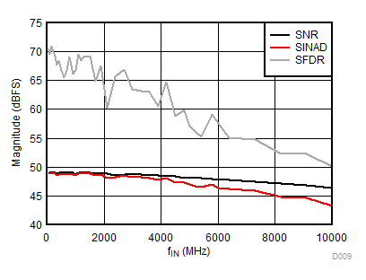
ADC08DJ3200 D009_SLVSDR1.gif
JMODE7, fS = 3200 MSPS, BG calibration
Figure 10. SNR, SINAD, SFDR vs Input Frequency
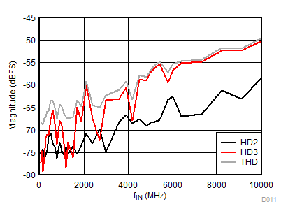
ADC08DJ3200 D011_SLVSDR1.gif
JMODE7, fS = 3200 MSPS, BG calibration
Figure 12. HD2, HD3, THD vs Input Frequency
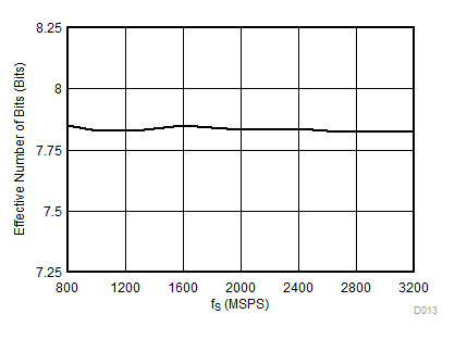
ADC08DJ3200 D013_SLVSDR1.gif
JMODE7, fIN = 347 MHz, BG calibration
Figure 14. ENOB vs Sampling Rate
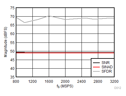
ADC08DJ3200 D012_SLVSDR1.gif
JMODE7, fIN = 347 MHz, BG calibration
Figure 16. SNR, SINAD, SFDR vs Sampling Rate
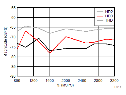
ADC08DJ3200 D014_SLVSDR1.gif
JMODE7, fIN = 347 MHz, BG calibration
Figure 18. HD2, HD3, THD vs Sampling Rate
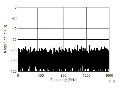
ADC08DJ3200 D139_SLVSDR1.gif
JMODE7, fIN = 350 MHz, FG calibration, SNR = 49.1 dBFS, SFDR = 70.1 dBFS, ENOB = 7.80 bits
Figure 20. Single-Tone FFT at AIN = –1 dBFS
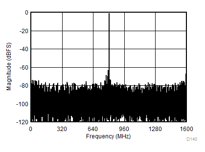
ADC08DJ3200 D140_SLVSDR1.gif
JMODE7, fIN = 2400 MHz, FG calibration, SNR = 48.8 dBFS, SFDR = 63.7 dBFS, ENOB = 7.74 bits
Figure 22. Single-Tone FFT at AIN = –1 dBFS
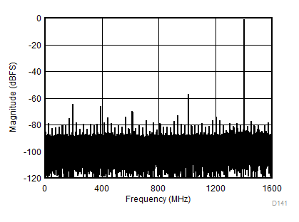
ADC08DJ3200 D141_SLVSDR1.gif
JMODE7, fIN = 5000 MHz, FG calibration, SNR = 48.4 dBFS, SFDR = 57.1 dBFS, ENOB = 7.52 bits
Figure 24. Single-Tone FFT at AIN = –1 dBFS
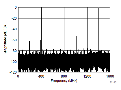
ADC08DJ3200 D145_SLVSDR1.gif
JMODE7, fIN = 8200 MHz, FG calibration, SNR = 47.4 dBFS, SFDR = 52.4 dBFS, ENOB = 7.19 bits
Figure 26. Single-Tone FFT at AIN = –1 dBFS
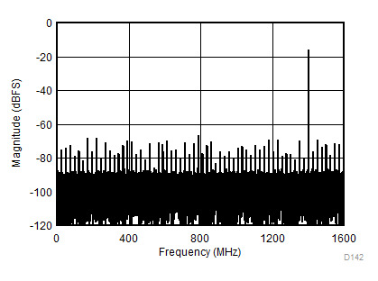
ADC08DJ3200 D142_SLVSDR1.gif
JMODE7, fIN = 8200 MHz, FG calibration, SNR = 49.2 dBFS, SFDR = 65.9 dBFS, ENOB = 7.80 bits
Figure 28. Single-Tone FFT at AIN = –16 dBFS
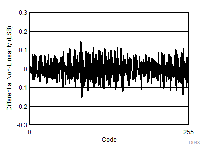
ADC08DJ3200 D048_SLVSDR1.gif
JMODE5, fS = 6400 MSPS, FG calibration
Figure 30. DNL vs Code
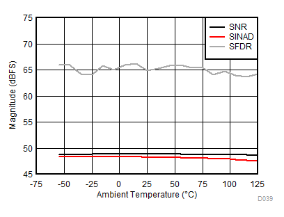
ADC08DJ3200 D039_SLVSDR1.gif
JMODE5, fS = 6400 MSPS, fIN = 2400 MHz, BG calibration
Figure 32. SNR, SINAD, SFDR vs Temperature
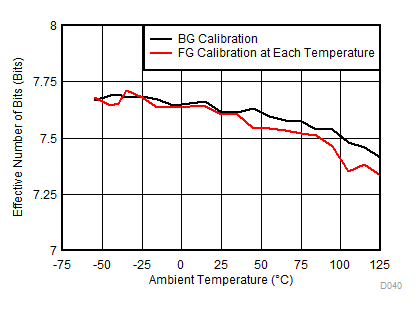
ADC08DJ3200 D040_SLVSDR1.gif
JMODE5, fIN = 2400 MHz, fS = 6400 MSPS
Figure 34. ENOB vs Temperature and Calibration Type
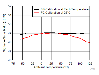
ADC08DJ3200 D063_SLVSDR1.gif
JMODE5, fIN = 600 MHz, fS = 6400 MSPS
Figure 36. SNR vs Temperature and Calibration Type
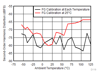
ADC08DJ3200 D119_SLVSDR1.gif
JMODE5, fIN = 600 MHz, fS = 6400 MSPS
Figure 38. HD2 vs Temperature and Calibration Type
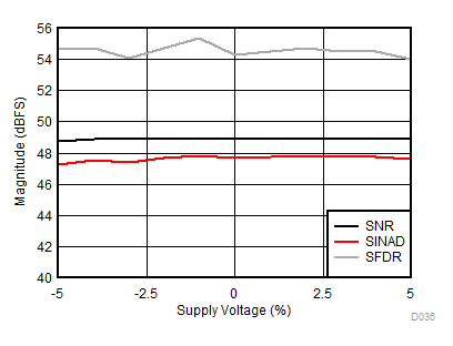
ADC08DJ3200 D036_SLVSDR1.gif
JMODE5, fS = 6400 MSPS, fIN = 2400 MHz, FG calibration
Figure 40. SNR, SINAD, SFDR vs Supply Voltage
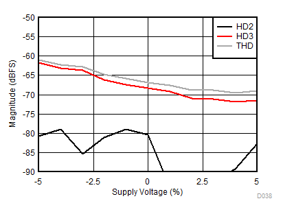
ADC08DJ3200 D038_SLVSDR1.gif
JMODE5, fS = 6400 MSPS, fIN = 2400 MHz, FG calibration
Figure 42. HD2, HD3, THD vs Supply Voltage
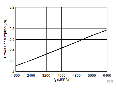
ADC08DJ3200 D008_SLVSDR1.gif
JMODE5, fIN = 347 MHz, FG calibration
Figure 44. Power Consumption vs Sampling Rate
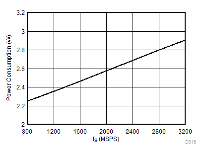
ADC08DJ3200 D016_SLVSDR1.gif
JMODE7, fIN = 347 MHz, FG calibration
Figure 46. Power Consumption vs Sampling Rate
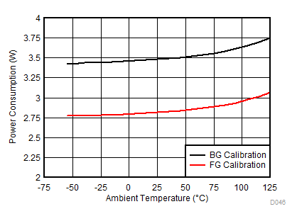
ADC08DJ3200 D046_SLVSDR1.gif
JMODE5, fS = 6400 MSPS, fIN = 2400 MHz, BG calibration
Figure 48. Power Consumption vs Temperature
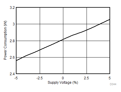
ADC08DJ3200 D044_SLVSDR1.gif
JMODE5, fS = 6400 MSPS, FG calibration
Figure 50. Power Consumption vs Supply Voltage
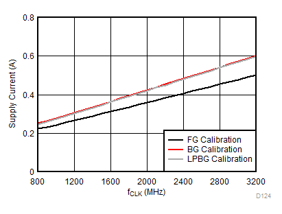
ADC08DJ3200 D124_SLVSDR1.gif
JMODE5, fIN = 607 MHz
Figure 52. IA11 Supply Current vs Clock Frequency
ADC08DJ3200 D118_SLVSDR1.gif
JMODE5, fIN = 607 MHz
Figure 54. Power Consumption vs Clock Frequency
ADC08DJ3200 D122_SLVSDR1.gif
fIN = 2400 MHz, fCLK = 3200 MHz, BG calibration
Figure 56. Supply Current vs JMODE
ADC08DJ3200 D125_SLVSDR1.gif
JMODE4, fCLK = 3200 MHz, fIN = 3199.9 MHz
Figure 58. Background Calibration Core Transition
(AC Signal)
ADC08DJ3200 D127_SLVSDR1.gif
JMODE4, fCLK = 3200 MHz, DC input
Figure 60. Background Calibration Core Transition
(DC Signal)
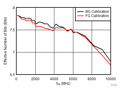
ADC08DJ3200 D002_SLVSDR1.gif
JMODE5, fS = 6400 MSPS, FG and BG calibration
Figure 5. ENOB vs Input Frequency
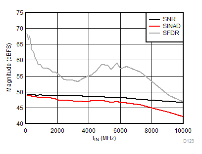
ADC08DJ3200 D129_SLVSDR1.gif
JMODE5, fS = 6400 MSPS, FG calibration
Figure 7. SNR, SINAD, SFDR vs Input Frequency
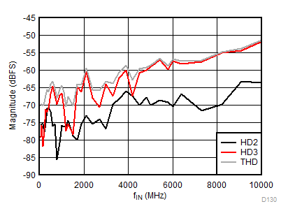
ADC08DJ3200 D130_SLVSDR1.gif
JMODE5, fS = 6400 MSPS, FG calibration
Figure 9. HD2, HD3, THD vs Input Frequency
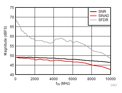
ADC08DJ3200 D001_SLVSDR1.gif
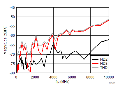
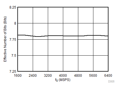
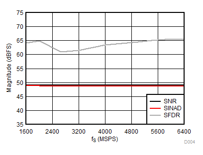
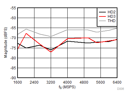
JMODE5, fS = 6400 MSPS, BG calibration
Figure 11. SNR, SINAD, SFDR vs Input Frequency
ADC08DJ3200 D003_SLVSDR1.gif
JMODE5, fS = 6400 MSPS, BG calibration
Figure 13. HD2, HD3, THD vs Input Frequency
ADC08DJ3200 D005_SLVSDR1.gif
JMODE5, fIN = 347 MHz, BG calibration
Figure 15. ENOB vs Sampling Rate
ADC08DJ3200 D004_SLVSDR1.gif
JMODE5, fIN = 347 MHz, BG calibration
Figure 17. SNR, SINAD, SFDR vs Sampling Rate
ADC08DJ3200 D006_SLVSDR1.gif
JMODE5, fIN = 347 MHz, BG calibration
Figure 19. HD2, HD3, THD vs Sampling Rate
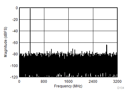
ADC08DJ3200 D134_SLVSDR1.gif
JMODE5, fIN = 350 MHz, FG calibration, SNR = 49.0 dBFS, SFDR = 64.0 dBFS, ENOB = 7.80 bits
Figure 21. Single-Tone FFT at AIN = –1 dBFS
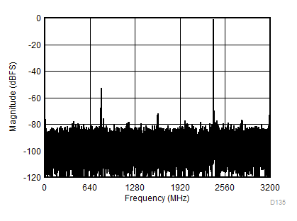
ADC08DJ3200 D135_SLVSDR1.gif
JMODE5, fIN = 2400 MHz, FG calibration, SNR = 48.8 dBFS, SFDR = 52.4 dBFS, ENOB = 7.53 bits
Figure 23. Single-Tone FFT at AIN = –1 dBFS
ADC08DJ3200 D136_SLVSDR1.gif
JMODE5, fIN = 5000 MHz, FG calibration, SNR = 48.3 dBFS, SFDR = 57.2 dBFS, ENOB = 7.48 bits
Figure 25. Single-Tone FFT at AIN = –1 dBFS
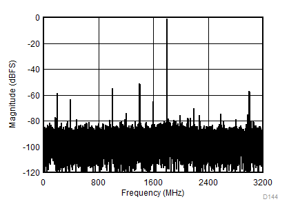
ADC08DJ3200 D144_SLVSDR1.gif
JMODE5, fIN = 8200 MHz, FG calibration, SNR = 47.4 dBFS, SFDR = 51.4 dBFS, ENOB = 7.10 bits
Figure 27. Single-Tone FFT at AIN = –1 dBFS
ADC08DJ3200 D137_SLVSDR1.gif
JMODE5, fIN = 8200 MHz, FG calibration, SNR = 49.0 dBFS, SFDR = 67.5 dBFS, ENOB = 7.79 bits
Figure 29. Single-Tone FFT at AIN = –16 dBFS
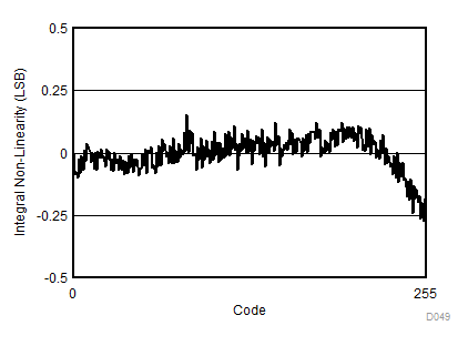
ADC08DJ3200 D049_SLVSDR1.gif
JMODE5, fS = 6400 MSPS, FG calibration
Figure 31. INL vs Code
ADC08DJ3200 D041_SLVSDR1.gif
JMODE5, fS = 6400 MSPS, fIN = 2400 MHz, BG calibration
Figure 33. HD2, HD3, THD vs Temperature
ADC08DJ3200 D121_SLVSDR1.gif
JMODE5, fIN = 600 MHz, fS = 6400 MSPS
Figure 35. ENOB vs Temperature and Calibration Type
ADC08DJ3200 D064_SLVSDR1.gif
JMODE5, fIN = 600 MHz, fS = 6400 MSPS
Figure 37. SFDR vs Temperature and Calibration Type
ADC08DJ3200 D120_SLVSDR1.gif
JMODE5, fIN = 600 MHz, fS = 6400 MSPS
Figure 39. HD3 vs Temperature and Calibration Type
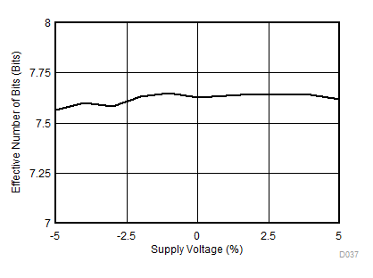
ADC08DJ3200 D037_SLVSDR1.gif
JMODE5, fS = 6400 MSPS, fIN = 2400 MHz, FG calibration
Figure 41. ENOB vs Supply Voltage
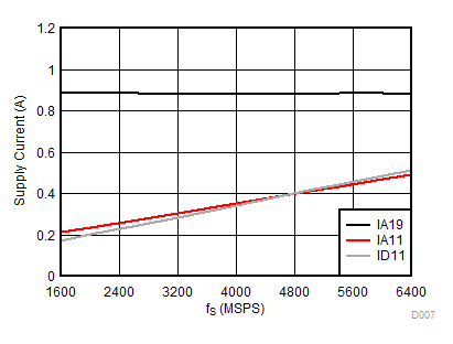
ADC08DJ3200 D007_SLVSDR1.gif
JMODE5, fIN = 347 MHz, FG calibration
Figure 43. Supply Current vs Sampling Rate
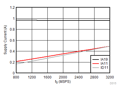
ADC08DJ3200 D015_SLVSDR1.gif
JMODE7, fIN = 347 MHz, FG calibration
Figure 45. Supply Current vs Sampling Rate
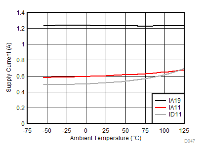
ADC08DJ3200 D047_SLVSDR1.gif
JMODE5, fS = 6400 MSPS, fIN = 2400 MHz, BG calibration
Figure 47. Supply Current vs Temperature
ADC08DJ3200 D045_SLVSDR1.gif
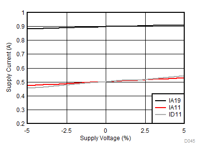
JMODE5, fS = 6400 MSPS, FG calibration
Figure 49. Supply Current vs Supply Voltage
ADC08DJ3200 D123_SLVSDR1.gif
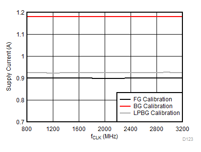
JMODE5, fIN = 607 MHz
Figure 51. IA19 Supply Current vs Clock Frequency
ADC08DJ3200 D117_SLVSDR1.gif
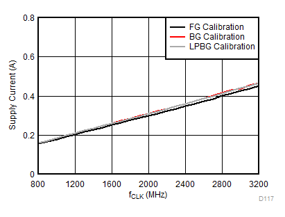
JMODE5, fIN = 607 MHz
Figure 53. ID11 Supply Current vs Clock Frequency
ADC08DJ3200 D034_SLVSDR1.gif
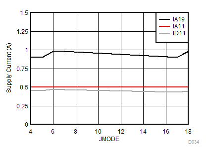
fIN = 2400 MHz, fCLK = 3200 MHz, FG calibration
Figure 55. Supply Current vs JMODE
ADC08DJ3200 D033_SLVSDR1.gif
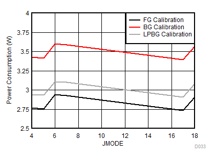
fIN = 2400 MHz, fCLK = 3200 MHz
Figure 57. Power Consumption vs JMODE
ADC08DJ3200 D126_SLVSDR1.gif
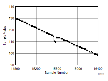
JMODE4, fCLK = 3200 MHz, fIN = 3199.9 MHz
Figure 59. Background Calibration Core Transition
(AC Signal Zoomed)
ADC08DJ3200 D128_SLVSDR1.gif
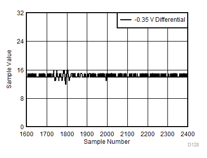
JMODE4, fCLK = 3200 MHz, DC input
Figure 61. Background Calibration Core Transition
(DC Signal Zoomed)