SNAS480N May 2010 – August 2015 ADC12D1000 , ADC12D1600
PRODUCTION DATA.
- 1 Features
- 2 Applications
- 3 Description
- 4 Revision History
- 5 Pin Configuration and Functions
-
6 Specifications
- 6.1 Absolute Maximum Ratings
- 6.2 ESD Ratings
- 6.3 Recommended Operating Conditions
- 6.4 Thermal Information
- 6.5 Electrical Characteristics: Static Converter
- 6.6 Electrical Characteristics: Dynamic Converter
- 6.7 Electrical Characteristics: Analog Input/Output and Reference
- 6.8 Electrical Characteristics: I-Channel To Q-Channel
- 6.9 Electrical Characteristics: Converter and Sampling Clock
- 6.10 Electrical Characteristics: Autosync Feature
- 6.11 Electrical Characteristics: Digital Control and Output Pin
- 6.12 Electrical Characteristics: Power Supply
- 6.13 Electrical Characteristics: AC
- 6.14 Timing Requirements: Serial Port Interface
- 6.15 Timing Requirements: Calibration
- 6.16 Typical Characteristics
-
7 Detailed Description
- 7.1 Overview
- 7.2 Functional Block Diagram
- 7.3 Feature Description
- 7.4 Device Functional Modes
- 7.5
Programming
- 7.5.1
Control Modes
- 7.5.1.1
Non-Extended Control Mode
- 7.5.1.1.1 Dual Edge Sampling Pin (DES)
- 7.5.1.1.2 Non-Demultiplexed Mode Pin (NDM)
- 7.5.1.1.3 Dual Data Rate Phase Pin (DDRPH)
- 7.5.1.1.4 Calibration Pin (CAL)
- 7.5.1.1.5 Calibration Delay Pin (CALDLY)
- 7.5.1.1.6 Power-Down I-Channel Pin (PDI)
- 7.5.1.1.7 Power-Down Q-Channel Pin (PDQ)
- 7.5.1.1.8 Test Pattern Mode Pin (TPM)
- 7.5.1.1.9 Full-Scale Input Range Pin (FSR)
- 7.5.1.1.10 AC-DC-Coupled Mode Pin (VCMO)
- 7.5.1.1.11 LVDS Output Common-Mode Pin (VBG)
- 7.5.1.2 Extended Control Mode
- 7.5.1.1
Non-Extended Control Mode
- 7.5.1
Control Modes
- 7.6 Register Maps
- 8 Application and Implementation
- 9 Power Supply Recommendations
- 10Layout
- 11Device and Documentation Support
- 12Mechanical, Packaging, and Orderable Information
Package Options
Mechanical Data (Package|Pins)
- NXA|292
Thermal pad, mechanical data (Package|Pins)
Orderable Information
9 Power Supply Recommendations
Data-converter-based systems draw sufficient transient current to corrupt their own power supplies if not adequately bypassed. A 10-μF capacitor must be placed within one inch (2.5 cm) of the device power pins for each supply voltage. A 0.1-μF capacitor must be placed as close as possible to each supply pin, preferably within 0.5 cm. Leadless chip capacitors are preferred due to their low-lead inductance.
As is the case with all high-speed converters, the ADC12D1600 device must be assumed to have little power supply noise-rejection. Any power supply used for digital circuitry in a system where a large amount of digital power is consumed must not be used to supply power to the ADC12D1600 device. If not a dedicated supply, the ADC supplies must be the same supply used for other analog circuitry.
9.1 System Power-On Considerations
There are a couple important topics to consider associated with the system power-on event including configuration and calibration, and the Data Clock.
9.1.1 Power-On, Configuration, and Calibration
Following the application of power to the ADC12D1x00, several events must take place before the output from the ADC12D1x00 is valid and at full performance; at least one full calibration must be executed with the device configured in the desired mode.
Following the application of power to the ADC12D1x00, there is a delay of tCalDly and then the Power-on Calibration is executed. This is why TI recommends setting the CalDly Pin through an external pullup or pulldown resistor. This ensures that the state of that input will be properly set at the same time that power is applied to the ADC and tCalDly will be a known quantity. For the purpose of this section, it is assumed that CalDly is set as recommended.
The Control Bits or Pins must be set or written to configure the ADC12D1x00 in the desired mode. This must take place through either Extended Control Mode or Non-ECM (Pin Control Mode) before subsequent calibrations will yield an output at full performance in that mode. Some examples of modes include DES/Non-DES Mode, Demux/Non-demux Mode, and Full-Scale Range.
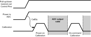
The simplest case is when device is in Non-ECM and the Control Pins are set by pullup and pulldown resistors, see Figure 75. For this case, the settings to the Control Pins ramp concurrently to the ADC voltage. Following the delay of tCalDly and the calibration execution time, tCAL, the output of the ADC12D1x00 is valid and at full performance. If it takes longer than tCalDly for the system to stabilize at its operating temperature, TI recommends executing an on-command calibration at that time.
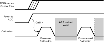
Another case is when the FPGA configures the Control Pins (Non-ECM) or writes to the SPI (ECM), see Figure 76. It is always necessary to comply with the Operating Ratings and Absolute Maximum ratings, that is, the Control Pins may not be driven below the ground or above the supply, regardless of what the voltage currently applied to the supply is. Therefore, it is not recommended to write to the Control Pins or SPI before power is applied to the ADC12D1x00. As long as the FPGA has completed writing to the Control Pins or SPI, the Power-on Calibration will result in a valid output at full performance. Once again, if it takes longer than tCalDly for the system to stabilize at its operating temperature, TI recommends executing an on-command calibration at that time.
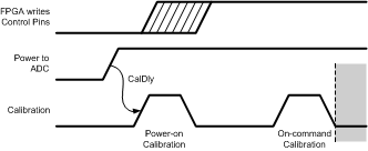
Due to system requirements, it may not be possible for the FPGA to write to the Control Pins or SPI before the Power-on Calibration takes place, see Figure 77. It is not critical to configure the device before the Power-on Calibration, but it is critical to realize that the output for such a case is not at its full performance. Following an On-command Calibration, the device will be at its full performance.
 Figure 75. Power-On With Control Pins Set by Pullup and Pulldown Resistors
 Figure 76. Power-On With Control Pins Set by FPGA Pre Power-on Cal
 Figure 77. Power-On With Control Pins Set by FPGA Post Power-on Cal
9.1.2 Power-On and Data Clock (Dclk)
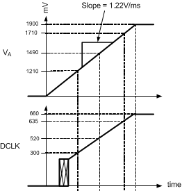
Many applications use the DCLK output for a system clock. For the ADC12D1x00, each I- and Q-channel has its own DCLKI and DCLKQ, respectively. The DCLK output is always active, unless that channel is powered-down or the DCLK Reset feature is used while the device is in Demux Mode. As the supply to the ADC12D1x00 ramps, the DCLK also comes up, see this example from the ADC12D1x00RB: Figure 78. While the supply is too low, there is no output at DCLK. As the supply continues to ramp, DCLK functions intermittently with irregular frequency, but the amplitude continues to track with the supply. Much below the low end of operating supply range of the ADC12D1x00, the DCLK is already fully operational.
 Figure 78. Supply and DCLK Ramping
9.2 Supply Voltage
The ADC12D1600 device is specified to operate with nominal supply voltages of 1.9 V (VA, VTC, VE and VDR). For detailed information regarding the operating voltage minimums and maximums see Recommended Operating Conditions.
The voltage on a pin (except VinI± and VinQ±), including a transient basis, must not have a voltage that is in excess of the supply voltage or below ground by more than 150 mV. A pin voltage that is higher than the supply or that is below ground can be a problem during start-up and shutdown of power. Ensure that the supplies to circuits driving any of the input pins, analog or digital, do not rise faster than the voltage at the ADC12D1600 power pins.
The values in Absolute Maximum Ratings must be strictly observed including during power up and power down. A power supply that produces a voltage spike at power turnon, turnoff, or both can destroy the ADC12D1600 device. Many linear regulators produce output spiking at power on unless there is a minimum load provided. Active devices draw very little current until the supply voltages reach a few hundred millivolts. The result can be a turnon spike that destroys the ADC12D1600 device, unless a minimum load is provided for the supply. A 100-Ω resistor at the regulator output provides a minimum output current during power up to ensure that no turnon spiking occurs. Whether a linear or switching regulator is used, TI recommends using a soft-start circuit to prevent overshoot of the supply.