SNAS717A April 2017 – October 2021 ADC12D1620QML-SP
PRODUCTION DATA
- 1 Features
- 2 Applications
- 3 Description
- 4 Revision History
- 5 Pin Configuration and Functions
-
6 Specifications
- 6.1 Absolute Maximum Ratings
- 6.2 ESD Ratings
- 6.3 Recommended Operating Conditions
- 6.4 Thermal Information
- 6.5 Converter Electrical Characteristics: Static Converter Characteristics
- 6.6 Converter Electrical Characteristics: Dynamic Converter Characteristics
- 6.7 Converter Electrical Characteristics: Analog Input/Output and Reference Characteristics
- 6.8 Converter Electrical Characteristic: Channel-to-Channel Characteristics
- 6.9 Converter Electrical Characteristics: LVDS CLK Input Characteristics
- 6.10 Electrical Characteristics: AutoSync Feature
- 6.11 Converter Electrical Characteristics: Digital Control and Output Pin Characteristics
- 6.12 Converter Electrical Characteristics: Power Supply Characteristics
- 6.13 Converter Electrical Characteristics: AC Electrical Characteristics
- 6.14 Electrical Characteristics: Delta Parameters
- 6.15 Timing Requirements: Serial Port Interface
- 6.16 Timing Requirements: Calibration
- 6.17 Quality Conformance Inspection
- 6.18 Timing Diagrams
- 6.19 Typical Characteristics
-
7 Detailed Description
- 7.1 Overview
- 7.2 Functional Block Diagram
- 7.3 Feature Description
- 7.4 Device Functional Modes
- 7.5
Programming
- 7.5.1
Control Modes
- 7.5.1.1
Non-ECM
- 7.5.1.1.1 Dual-Edge Sampling Pin (DES)
- 7.5.1.1.2 Non-Demultiplexed Mode Pin (NDM)
- 7.5.1.1.3 Dual Data-Rate Phase Pin (DDRPh)
- 7.5.1.1.4 Calibration Pin (CAL)
- 7.5.1.1.5 Low-Sampling Power-Saving Mode Pin (LSPSM)
- 7.5.1.1.6 Power-Down I-Channel Pin (PDI)
- 7.5.1.1.7 Power-Down Q-Channel Pin (PDQ)
- 7.5.1.1.8 Test-Pattern Mode Pin (TPM)
- 7.5.1.1.9 Full-Scale Input-Range Pin (FSR)
- 7.5.1.1.10 AC- or DC-Coupled Mode Pin (VCMO)
- 7.5.1.1.11 LVDS Output Common-Mode Pin (VBG)
- 7.5.1.2 Extended Control Mode
- 7.5.1.1
Non-ECM
- 7.5.1
Control Modes
- 7.6 Register Maps
- 8 Application Information Disclaimer
- 9 Power Supply Recommendations
- 10Layout
- 11Device and Documentation Support
- 12Mechanical, Packaging, and Orderable Information
Package Options
Refer to the PDF data sheet for device specific package drawings
Mechanical Data (Package|Pins)
- FVA|256
- NAA|376
Thermal pad, mechanical data (Package|Pins)
Orderable Information
3 Description
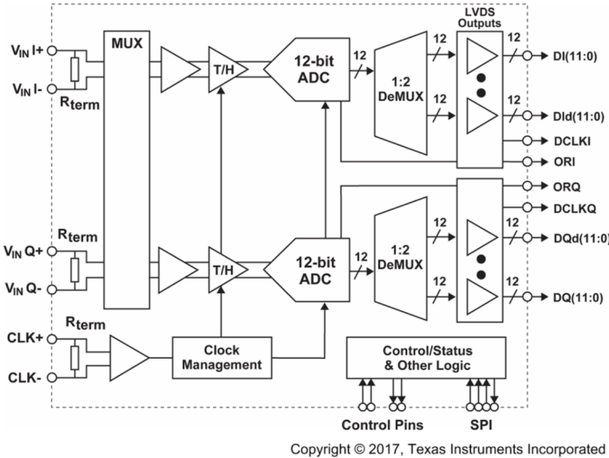
The ADC12D1620QML uses a package redesign to achieve better ENOB, SNR, and X-talk compared to the ADC12D1600QML. As is its predecessor, the ADC12D1620QML is a low-power, high-performance CMOS analog-to-digital converter (ADC) that digitizes signals at a 12-bit resolution at sampling rates up to 3.2 GSPS in an interleaved mode. It can also be used as a dual-channel ADC for sampling rates up to 1.6 GSPS. For sampling rates below 800 MHz, there is a low-sampling power-saving mode (LSPSM) that reduces power consumption to less than 1.4 W per channel (typical). The ADC can support conversion rates as low as 200 MSPS.
| PART NUMBER(1) | GRADE | PACKAGE |
|---|---|---|
| 5962F1220502VXF | SMD Flight 300 krad(Si) | CCGA (376) |
| ADC12D1620CCMLS | Flight 300 krad(Si) | CCGA (376) |
| ADC12D1620CCMPR | Pre-flight engineering prototype | CCGA (376) |
| ADC10D1000DAISY | Daisy chain, mechanical sample, no die | CCGA (376) |
| ADC12D1620LGMLS | Flight 300 krad(Si) | CLGA (256) |
| ADC12D1620LGMPR | Pre-flight engineering prototype | CLGA (256) |
| ADC10D1000LDAZ | Daisy chain, mechanical sample, no die | CLGA (256) |
 Functional Block Diagram