SLVSDR2B November 2018 – March 2021 ADC12DJ3200QML-SP
PRODUCTION DATA
- 1 Features
- 2 Applications
- 3 Description
- 4 Revision History
- 5 Pin Configuration and Functions
-
6 Specifications
- 6.1 Absolute Maximum Ratings
- 6.2 ESD Ratings
- 6.3 Recommended Operating Conditions
- 6.4 Thermal Information
- 6.5 Electrical Characteristics: DC Specifications
- 6.6 Electrical Characteristics: Power Consumption
- 6.7 Electrical Characteristics: AC Specifications (Dual-Channel Mode)
- 6.8 Electrical Characteristics: AC Specifications (Single-Channel Mode)
- 6.9 Timing Requirements
- 6.10 Switching Characteristics
- 6.11 Timing Diagrams
- 6.12 Typical Characteristics
-
7 Detailed Description
- 7.1 Overview
- 7.2 Functional Block Diagram
- 7.3
Feature Description
- 7.3.1 Analog Inputs
- 7.3.2 ADC Core
- 7.3.3 Timestamp
- 7.3.4 Clocking
- 7.3.5 Digital Down Converters (Dual-Channel Mode Only)
- 7.3.6 JESD204B Interface
- 7.3.7 Alarm Monitoring
- 7.3.8 Temperature Monitoring Diode
- 7.3.9 Analog Reference Voltage
- 7.4
Device Functional Modes
- 7.4.1 Dual-Channel Mode
- 7.4.2 Single-Channel Mode (DES Mode)
- 7.4.3 JESD204B Modes
- 7.4.4 Power-Down Modes
- 7.4.5 Test Modes
- 7.4.6 Calibration Modes and Trimming
- 7.4.7 Offset Calibration
- 7.4.8 Trimming
- 7.4.9 Offset Filtering
- 7.5 Programming
- 7.6 Register Maps
- 8 Application Information Disclaimer
- 9 Layout
- 10Device and Documentation Support
Package Options
Refer to the PDF data sheet for device specific package drawings
Mechanical Data (Package|Pins)
- ZMX|196
- NWE|196
Thermal pad, mechanical data (Package|Pins)
Orderable Information
7.3.4 Clocking
The clocking subsystem of the ADC12DJ3200QML-SP has two input signals, device clock (CLK+, CLK–) and SYSREF (SYSREF+, SYSREF–). Within the clocking subsystem there is a noiseless aperture delay adjustment (tAD adjust), a clock duty cycle corrector, and a SYSREF capture block. Figure 7-3 shows the clocking subsystem.
 Figure 7-3 ADC12DJ3200QML-SP Clocking Subsystem
The device clock is used as the sampling clock for the ADC core as well as the clocking for the digital processing and serializer outputs. Use a low-noise (low jitter) device clock to maintain high signal-to-noise ratio (SNR) within the ADC. In dual-channel mode, the analog input signal for each input is sampled on the rising edge of the device clock. In single-channel mode, both the rising and falling edges of the device clock are used to capture the analog signal to reduce the maximum clock rate required by the ADC. A noiseless aperture delay adjustment (tAD adjust) allows the user to shift the sampling instance of the ADC in fine steps in order to synchronize multiple ADC12DJ3200QML-SPs or to fine-tune system latency. Duty cycle correction is implemented in the ADC12DJ3200QML-SP to ease the requirements on the external device clock while maintaining high performance. Table 7-4 summarizes the device clock interface in dual-channel mode and single-channel mode.
| MODE OF OPERATION | SAMPLING RATE VS fCLK | SAMPLING INSTANT |
|---|---|---|
| Dual-channel mode | 1 × fCLK | Rising edge |
| Single-channel mode | 2 × fCLK | Rising and falling edge |
SYSREF is a system timing reference used for JESD204B subclass-1 implementations of deterministic latency. SYSREF is used to achieve deterministic latency and for multi-device synchronization. SYSREF must be captured by the correct device clock edge in order to achieve repeatable latency and synchronization. The ADC12DJ3200QML-SP includes SYSREF windowing and automatic SYSREF calibration to ease the requirements on the external clocking circuits and to simplify the synchronization process. SYSREF can be implemented as a single pulse or as a periodic clock. In periodic implementations, SYSREF must be equal to, or an integer division of, the local multiframe clock frequency. Equation 2 is used to calculate valid SYSREF frequencies.
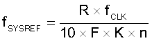
where
- R and F are set by the JMODE setting (see Table 7-18)
- fCLK is the device clock frequency (CLK±)
- K is the programmed multiframe length (see Table 7-18 for valid K settings)
- and n is any positive integer