SLAS989D January 2014 – October 2017 ADC12J4000
PRODUCTION DATA.
- 1 Features
- 2 Applications
- 3 Description
- 4 Revision History
- 5 Pin Configuration and Functions
- 6 Specifications
-
7 Detailed Description
- 7.1 Overview
- 7.2 Functional Block Diagram
- 7.3
Feature Description
- 7.3.1 Signal Acquisition
- 7.3.2 The Analog Inputs
- 7.3.3 Clocking
- 7.3.4 Over-Range Function
- 7.3.5 ADC Core Features
- 7.3.6
Digital Down Converter (DDC)
- 7.3.6.1 NCO/Mixer
- 7.3.6.2 NCO Settings
- 7.3.6.3 Decimation Filters
- 7.3.6.4 DDC Output Data
- 7.3.6.5 Decimation Settings
- 7.3.7
Data Outputs
- 7.3.7.1 The Digital Outputs
- 7.3.7.2
JESD204B Interface Features and Settings
- 7.3.7.2.1 Scrambler Enable
- 7.3.7.2.2 Frames Per Multi-Frame (K-1)
- 7.3.7.2.3 DDR
- 7.3.7.2.4 JESD Enable
- 7.3.7.2.5 JESD Test Modes
- 7.3.7.2.6 Configurable Pre-Emphasis
- 7.3.7.2.7 Serial Output-Data Formatting
- 7.3.7.2.8 JESD204B Synchronization Features
- 7.3.7.2.9 SYSREF
- 7.3.7.2.10 SYNC~
- 7.3.7.2.11 Time Stamp
- 7.3.7.2.12 Code-Group Synchronization
- 7.3.7.2.13 Multiple ADC Synchronization
- 7.4 Device Functional Modes
- 7.5 Programming
- 7.6
Register Map
- 7.6.1 Memory Map
- 7.6.2
Register Descriptions
- 7.6.2.1
Standard SPI-3.0 (0x000 to 0x00F)
- 7.6.2.1.1 Configuration A Register (address = 0x000) [reset = 0x3C]
- 7.6.2.1.2 Configuration B Register (address = 0x001) [reset = 0x00]
- 7.6.2.1.3 Device Configuration Register (address = 0x002) [reset = 0x00]
- 7.6.2.1.4 Chip Type Register (address = 0x003) [reset = 0x03]
- 7.6.2.1.5 Chip Version Register (address = 0x006) [reset = 0x13]
- 7.6.2.1.6 Vendor Identification Register (address = 0x00C to 0x00D) [reset = 0x0451]
- 7.6.2.2 User SPI Configuration (0x010 to 0x01F)
- 7.6.2.3
General Analog, Bias, Band Gap, and Track and Hold (0x020 to 0x02F)
- 7.6.2.3.1 Power-On Reset Register (address = 0x021) [reset = 0x00]
- 7.6.2.3.2 I/O Gain 0 Register (address = 0x022) [reset = 0x40]
- 7.6.2.3.3 IO_GAIN_1 Register (address = 0x023) [reset = 0x00]
- 7.6.2.3.4 I/O Offset 0 Register (address = 0x025) [reset = 0x40]
- 7.6.2.3.5 I/O Offset 1 Register (address = 0x026) [reset = 0x00]
- 7.6.2.4
Clock (0x030 to 0x03F)
- 7.6.2.4.1 Clock Generator Control 0 Register (address = 0x030) [reset = 0xC0]
- 7.6.2.4.2 Clock Generator Status Register (address = 0x031) [reset = 0x07]
- 7.6.2.4.3 Clock Generator Control 2 Register (address = 0x032) [reset = 0x80]
- 7.6.2.4.4 Analog Miscellaneous Register (address = 0x033) [reset = 0xC3]
- 7.6.2.4.5 Input Clamp Enable Register (address = 0x034) [reset = 0x2F]
- 7.6.2.5 Serializer (0x040 to 0x04F)
- 7.6.2.6
ADC Calibration (0x050 to 0x1FF)
- 7.6.2.6.1 Calibration Configuration 0 Register (address = 0x050) [reset = 0x06]
- 7.6.2.6.2 Calibration Configuration 1 Register (address = 0x051) [reset = 0xF4]
- 7.6.2.6.3 Calibration Background Control Register (address = 0x057) [reset = 0x10]
- 7.6.2.6.4 ADC Pattern and Over-Range Enable Register (address = 0x058) [reset = 0x00]
- 7.6.2.6.5 Calibration Vectors Register (address = 0x05A) [reset = 0x00]
- 7.6.2.6.6 Calibration Status Register (address = 0x05B) [reset = undefined]
- 7.6.2.6.7 Timing Calibration Register (address = 0x066) [reset = 0x02]
- 7.6.2.7
Digital Down Converter and JESD204B (0x200-0x27F)
- 7.6.2.7.1 Digital Down-Converter (DDC) Control Register (address = 0x200) [reset = 0x10]
- 7.6.2.7.2 JESD204B Control 1 Register (address = 0x201) [reset = 0x0F]
- 7.6.2.7.3 JESD204B Control 2 Register (address = 0x202) [reset = 0x00]
- 7.6.2.7.4 JESD204B Device ID (DID) Register (address = 0x203) [reset = 0x00]
- 7.6.2.7.5 JESD204B Control 3 Register (address = 0x204) [reset = 0x00]
- 7.6.2.7.6 JESD204B and System Status Register (address = 0x205) [reset = Undefined]
- 7.6.2.7.7 Overrange Threshold 0 Register (address = 0x206) [reset = 0xF2]
- 7.6.2.7.8 Overrange Threshold 1 Register (address = 0x207) [reset = 0xAB]
- 7.6.2.7.9 Overrange Period Register (address = 0x208) [reset = 0x00]
- 7.6.2.7.10 DDC Configuration Preset Mode Register (address = 0x20C) [reset = 0x00]
- 7.6.2.7.11 DDC Configuration Preset Select Register (address = 0x20D) [reset = 0x00]
- 7.6.2.7.12 Rational NCO Reference Divisor Register (address = 0x20E to 0x20F) [reset = 0x0000]
- 7.6.2.7.13 NCO Frequency (Preset x) Register (address = see ) [reset = see ]
- 7.6.2.7.14 NCO Phase (Preset x) Register (address = see ) [reset = see ]
- 7.6.2.7.15 DDC Delay (Preset x) Register (address = see ) [reset = see ]
- 7.6.2.1
Standard SPI-3.0 (0x000 to 0x00F)
- 8 Application and Implementation
- 9 Power Supply Recommendations
- 10Layout
- 11Device and Documentation Support
- 12Mechanical, Packaging, and Orderable Information
Package Options
Mechanical Data (Package|Pins)
- NKE|68
Thermal pad, mechanical data (Package|Pins)
Orderable Information
8 Application and Implementation
NOTE
Information in the following applications sections is not part of the TI component specification, and TI does not warrant its accuracy or completeness. TI’s customers are responsible for determining suitability of components for their purposes. Customers should validate and test their design implementation to confirm system functionality.
8.1 Application Information
The ADC12J4000 device is a wideband sampling and digital tuning device. The ADC input captures input signals from DC to greater than 3 GHz. The DDC performs digital-down conversion and programmable decimation filtering, and outputs complex (15 bit I and 15 bit Q) data. In DDC Bypass Mode (Decimation = 1) the raw 12 bit ADC data is also available. The resulting output data is output on the JESD204B data interface for capture by the downstream capture or processing device. Most frequency-domain applications benefit from DDC capability to select the desired frequency band and provide only the necessary bandwidth of output data, minimizing the required number of data signals. Time domain applications generally require the raw 12-bit ADC output data provided by the DDC bypass feature.
8.2 Typical Application
8.2.1 RF Sampling Receiver
An RF Sampling Receiver is used to directly sample a signal in the RF frequency range and provide the data for the captured signal to downstream processing. The wide input bandwidth, high sampling rate, and DDC features of the ADC12J4000 make it ideally suited for this application.
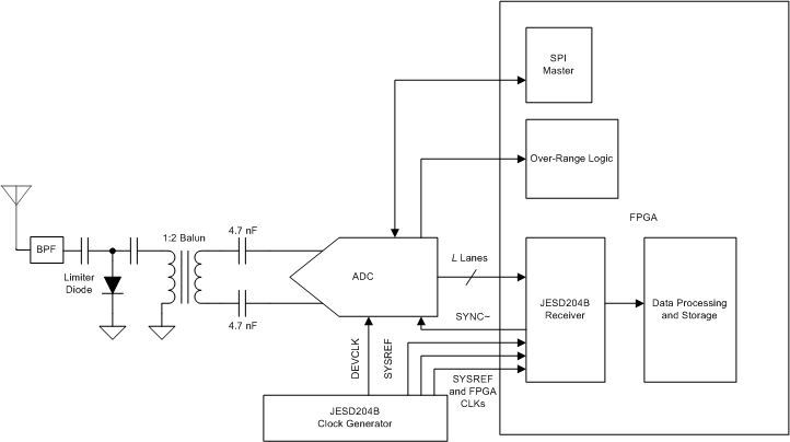 Figure 94. Simplified Schematic
8.2.1.1 Design Requirements
For this design example, use the parameters listed in Table 87.
Table 87. Design Parameters
| DESIGN PARAMETERS | EXAMPLE VALUES |
|---|---|
| Signal center frequency | 2500 MHz |
| Signal bandwidth | 100 MHz |
| Signal nominal amplitude | –7 dBm |
| Signal maximum amplitude | 6 dBm |
| Minimum SINAD (in bandwidth of interest) | 48 dBc |
| Minimum SFDR (in bandwidth of interest) | 60 dBc |
8.2.1.2 Detailed Design Procedure
Use the following steps to design the RF receiver:
- Use the signal-center frequency and signal bandwidth to select an appropriate sampling rate (DEVCLK frequency) and decimate factor (x / 4 to x / 32).
- Select the sampling rate so that the band of interest is completely within a Nyquist zone.
- Select the sampling rate so that the band of interest is away from any harmonics or interleaving tones.
- Use a frequency planning tool, such as the ADC harmonic calculator (see the Development Support section).
- Select the decimation factor that provides the highest factor possible with an adequate alias-protected output bandwidth to capture the frequency bandwidth of interest.
- Select other system components to provide the needed signal frequency range and DEVCLK rate.
- See Table 1 for recommended balun components.
- Select bandpass filters and limiter components based on the requirement to attenuate unwanted signals outside the band of interest (blockers) and to prevent large signals from damaging the ADC inputs. See the Absolute Maximum Ratings table.
The LMK048xx JESD204B clocking devices can provide the DEVCLK clock and other system clocks for ƒ(DEVCLK) < 3101 MHz.
For DEVCLK frequencies up to 4 GHz the consider using the LMX2581 and TRF3765 devices as the DEVCLK source. Use the LMK048xx device to provide the JESD204B clocks. For additional device information, see the Related Documentation section.
8.2.1.3 Application Curves
The following curves show an RF signal at 2497.97 MHz captured at a sample rate of 4000 MSPS. Figure 95 shows the spectrum for the full Nyquist band. Figure 96 shows the spectrum for the output data in decimate-by-32 mode with ƒ(NCO) equal to 2500 MHz. Figure 96 shows the ability to provide only the spectrum of interest in the decimated output data. Figure 96 also shows how proper selection of the sampling rate can ensure interleaving tones are outside the band of interest and outside the decimated frequency range. Lastly, Figure 96 shows the reduction in the noise floor provided by the processing gain of decimation.
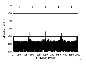
| DDC Bypass Mode | ƒS = 4000 MSPS | |
| FIN = 2497.97 MHz at –7 dBFS | ||
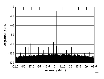
| ƒS = 4000 MSPS | ƒ(NCO) = 2500 MHz | |
| FIN = 2497.97 MHz at –7 dBFS | ||
8.2.2 Oscilloscope
The ADC12J4000 device is equally well-suited for high-speed time-domain applications such as oscilloscopes. The following typical application is for a generic high-speed oscilloscope. Adjustable gain is provided by the front-end resistor ladder and selection mux, and the gain adjustments of the LMH6518 device. Additional gain fine-tuning can be achieved using the full-scale range adjustment features of the ADC.
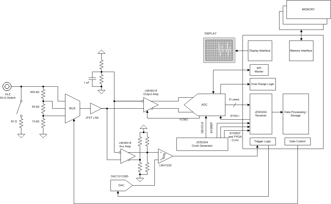 Figure 97. Simplified Schematic for an Oscilloscope
8.2.2.1 Design Requirements
For this design example, use the parameters listed in Table 88.
Table 88. Design Parameters
| DESIGN PARAMETERS | EXAMPLE VALUES |
|---|---|
| Maximum sample rate | 4000 MSPS |
| Maximum input frequency | 1500 MHz |
| 1-dB flat-frequency range | 0 to 1000 MHz |
| Signal maximum amplitude | 6 dBm |
| Signal minimum amplitude | 48 dBc |
| Maximum capture depth | 1 million points |
8.2.2.2 Detailed Design Procedure
Use the following primary steps to design a 12-bit oscilloscope:
- Select the desired sampling rate based on the maximum sampling-rate requirement.
- Select the input path components (LNA, amplifier, and other components) based on the maximum input frequency and 1-dB flat-frequency range requirements.
- Set the attenuation range steps based on the required minimum and maximum values for the signal amplitude.
- Select the memory size based on the resolution of the ADC output (12 bits) and the required maximum number of sample points.
8.2.2.3 Application Curves
The following curves show the time-domain sample data for a 150-MHz input signal at –1 dBFS, sampled at 4000 MSPS using the ADC12J4000 device. Figure 98 shows the raw time-domain data. Figure 99 shows the spectrum of the captured signal which shows the additional capability of a 12-bit ADC oscilloscope to provide basic spectrum-analysis functions with reasonable performance.
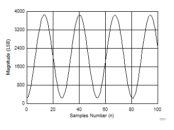
| FIN = 147.97 MHz at –1 dBFS | ƒS = 4000 MSPS | |
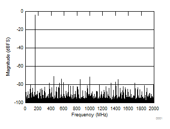
| FIN = 149.97 MHz at –1 dBFS | ƒS = 4000 MSPS | |
8.3 Initialization Set-Up
8.3.1 JESD204B Startup Sequence
The JESD204B interface requires a specific startup and alignment sequence. The general order of that sequence is listed in the following steps.
- Power up or reset the ADC12J4000 device.
- Program JESD_EN = 0 to shut down the link and enable configuration changes.
- Program DECIMATE, SCRAM_EN, KM1 and DDR to the desired settings.
- Configure the device calibration settings as desired, and initiate a calibration (set CAL_SFT = 1).
- Program JESD_EN = 1 to enable the link.
- Apply at least one SYSREF rising edge to establish the LMFC phase.
- Assert SYNC~ from the data receiver to initiate link communications.
- After the JESD204B receiver has established code group synchronization, SYNC~ is de-asserted and the ILA process begins.
- Immediately following the end of the ILA sequence normal data output begins.
NOTE
If deterministic latency is not required this step can be omitted.
8.4 Dos and Don'ts
8.4.1 Common Application Pitfalls
Driving the inputs (analog or digital) beyond the power supply rails. For device reliability, an input must not go more than 150 mV below the ground pins or 150 mV above the supply pins. Exceeding these limits even on a transient basis can cause faulty, or erratic, operation and can impair device reliability. High-speed digital circuits exhibiting undershoot that goes more than a volt below ground is common. To control overshoot, the impedance of high-speed lines must be controlled and these lines must be terminated in the characteristic impedance.
Care must be taken not to overdrive the inputs of the ADC12J4000 device. Such practice can lead to conversion inaccuracies and even to device damage.
Incorrect analog input common-mode voltage in the DC-coupled mode. As described in the The Analog Inputs and DC Coupled Input Usage sections, the input common-mode voltage (VCMI) must remain the specified range as referenced to the VCMO pin, which has a variability with temperature that must also be tracked. Distortion performance is degraded if the input common mode voltage is outside the specified VCMI range.
Using an inadequate amplifier to drive the analog input. Use care when choosing a high frequency amplifier to drive the ADC12J4000 device because many high-speed amplifiers have higher distortion than the ADC12J4000 device which results in overall system performance degradation.
Driving the clock input with an excessively high level signal. The ADC input clock level must not exceed the level described in the Recommended Operating Conditions table because the input offset can change if these levels are exceeded.
Inadequate input clock levels. As described in the Using the Serial Interface section, insufficient input clock levels can result in poor performance. Excessive input-clock levels can result in the introduction of an input offset.
Using a clock source with excessive jitter, using an excessively long input clock signal trace, or having other signals coupled to the input clock signal trace. These pitfalls cause the sampling interval to vary which causes excessive output noise and a reduction in SNR performance.
Failure to provide adequate heat removal. As described in the Thermal Management section, providing adequate heat removal is important to ensure device reliability. Adequate heat removal is primarily provided by properly connecting the thermal pad to the circuit board ground planes. Multiple vias should be arranged in a grid pattern in the area of the thermal pad. These vias will connect the topside pad to the internal ground planes and to a copper pour area on the opposite side of the printed circuit board.