SBAS670B July 2014 – April 2017 ADC3441 , ADC3442 , ADC3443 , ADC3444
PRODUCTION DATA.
- 1 Features
- 2 Applications
- 3 Description
- 4 Revision History
- 5 Device Comparison Table
- 6 Pin Configuration and Functions
-
7 Specifications
- 7.1 Absolute Maximum Ratings
- 7.2 ESD Ratings
- 7.3 Recommended Operating Conditions
- 7.4 Thermal Information
- 7.5 Electrical Characteristics: General
- 7.6 Electrical Characteristics: ADC3441, ADC3442
- 7.7 Electrical Characteristics: ADC3443, ADC3444
- 7.8 AC Performance: ADC3441
- 7.9 AC Performance: ADC3442
- 7.10 AC Performance: ADC3443
- 7.11 AC Performance: ADC3444
- 7.12 Digital Characteristics
- 7.13 Timing Requirements: General
- 7.14 Timing Requirements: LVDS Output
- 7.15 Typical Characteristics: ADC3441
- 7.16 Typical Characteristics: ADC3442
- 7.17 Typical Characteristics: ADC3443
- 7.18 Typical Characteristics: ADC3444
- 7.19 Typical Characteristics: Common
- 7.20 Typical Characteristics: Contour
- 8 Parameter Measurement Information
-
9 Detailed Description
- 9.1 Overview
- 9.2 Functional Block Diagram
- 9.3 Feature Description
- 9.4 Device Functional Modes
- 9.5 Programming
- 9.6
Register Maps
- 9.6.1
Serial Register Description
- 9.6.1.1 Register 01h (address = 01h)
- 9.6.1.2 Register 03h (address = 03h)
- 9.6.1.3 Register 04h (address = 04h)
- 9.6.1.4 Register 05h (address = 05h)
- 9.6.1.5 Register 06h (address = 06h)
- 9.6.1.6 Register 07h (address = 07h)
- 9.6.1.7 Register 09h (address = 09h)
- 9.6.1.8 Register 0Ah (address = 0Ah)
- 9.6.1.9 Register 0Bh (address = 0Bh)
- 9.6.1.10 Register 13h (address = 13h)
- 9.6.1.11 Register 0Eh (address = 0Eh)
- 9.6.1.12 Register 0Fh (address = 0Fh)
- 9.6.1.13 Register 15h (address = 15h)
- 9.6.1.14 Register 25h (address = 25h)
- 9.6.1.15 Register 27h (address = 27h)
- 9.6.1.16 Register 11Dh (address = 11Dh)
- 9.6.1.17 Register 122h (address = 122h)
- 9.6.1.18 Register 134h (address = 134h)
- 9.6.1.19 Register 139h (address = 139h)
- 9.6.1.20 Register 21Dh (address = 21Dh)
- 9.6.1.21 Register 222h (address = 222h)
- 9.6.1.22 Register 234h (address = 234h)
- 9.6.1.23 Register 239h (address = 239h)
- 9.6.1.24 Register 308h (address = 308h)
- 9.6.1.25 Register 41Dh (address = 41Dh)
- 9.6.1.26 Register 422h (address = 422h)
- 9.6.1.27 Register 434h (address = 434h)
- 9.6.1.28 Register 439h (address = 439h)
- 9.6.1.29 Register 51Dh (address = 51Dh)
- 9.6.1.30 Register 522h (address = 522h)
- 9.6.1.31 Register 534h (address = 534h)
- 9.6.1.32 Register 539h (address = 539h)
- 9.6.1.33 Register 608h (address = 608h)
- 9.6.1.34 Register 70Ah (address = 70Ah)
- 9.6.1
Serial Register Description
- 10Applications and Implementation
- 11Power Supply Recommendations
- 12Layout
- 13Device and Documentation Support
- 14Mechanical, Packaging, and Orderable Information
Package Options
Mechanical Data (Package|Pins)
- RTQ|56
Thermal pad, mechanical data (Package|Pins)
- RTQ|56
Orderable Information
10 Applications and Implementation
NOTE
Information in the following applications sections is not part of the TI component specification, and TI does not warrant its accuracy or completeness. TI’s customers are responsible for determining suitability of components for their purposes. Customers should validate and test their design implementation to confirm system functionality.
10.1 Application Information
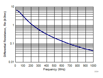
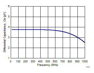
Typical applications involving transformer-coupled circuits are discussed in this section. Transformers (such as ADT1-1WT or WBC1-1) may be used up to 250 MHz to achieve good phase and amplitude balances at ADC inputs. While designing the dc driving circuits, the ADC input impedance must be considered. Figure 195 and Figure 196 show the impedance (Zin = Rin || Cin) across the ADC input pins.
 Figure 195. Differential Input Resistance, RIN
 Figure 196. Differential Input Capacitance, CIN
10.2 Typical Applications
10.2.1 Driving Circuit Design: Low Input Frequencies
 Figure 197. Driving Circuit for Low Input Frequencies
10.2.1.1 Design Requirements
For optimum performance, the analog inputs must be driven differentially. An optional 5-Ω to 15-Ω resistor in series with each input pin may be kept to damp out ringing caused by package parasitic. The drive circuit may have to be designed to minimize the impact of kick-back noise generated by sampling switches opening and closing inside the ADC, as well as ensuring low insertion loss over the desired frequency range and matched impedance to the source.
10.2.1.2 Detailed Design Procedure
A typical application involving using two back-to-back coupled transformers is shown in Figure 197. The circuit is optimized for low input frequencies. An external R-C-R filter using 50-Ω resistors and a 22-pF capacitor is used with the series inductor (39 nH), this combination helps absorb the sampling glitches. To improve phase and amplitude balance of first transformer, the termination resistors can be split between two transformers. For example, 25-Ω to 25-Ω termination across the secondary winding of the second transformer can be changed to 50-Ω to 50-Ω termination and another 50-Ω to 50-Ω resistor can be placed inside the dashed box between the transformers in Figure 197.
10.2.1.3 Application Curve
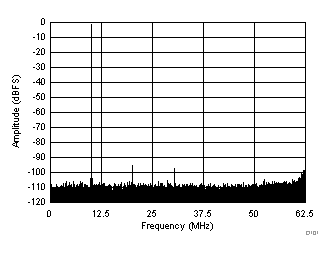
Figure 198 shows the performance obtained by using the circuit shown in Figure 197.
10.2.2 Driving Circuit Design: Input Frequencies Between 100 MHz to 230 MHz
 Figure 199. Driving Circuit for Mid-Range Input Frequencies (100 MHz < fIN < 230 MHz)
10.2.2.1 Design Requirements
See the Design Requirements section for further details.
10.2.2.2 Detailed Design Procedure
When input frequencies are between 100 MHz to 230 MHz, an R-LC-R circuit may be used to optimize performance, as shown in Figure 199.
10.2.2.3 Application Curve
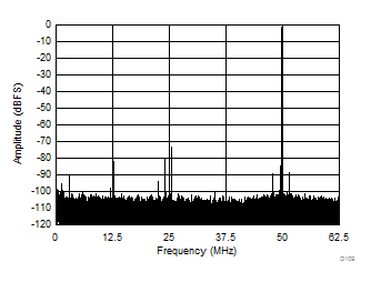
Figure 200 shows the performance obtained by using the circuit shown in Figure 199.
10.2.3 Driving Circuit Design: Input Frequencies Greater than 230 MHz
 Figure 201. Driving Circuit for High Input Frequencies (fIN > 230 MHz)
10.2.3.1 Design Requirements
See the Design Requirements section for further details.
10.2.3.2 Detailed Design Procedure
For high input frequencies (> 230 MHz), using the R-C-R or R-LC-R circuit does not show significant improvement in performance. However, a series resistance of 10 Ω may be used as shown in Figure 201.
10.2.3.3 Application Curve
Figure 202 shows the performance obtained by using the circuit shown in Figure 201.


