SBAS664B May 2014 – November 2014 ADC34J42 , ADC34J43 , ADC34J44 , ADC34J45
PRODUCTION DATA.
- 1 Features
- 2 Applications
- 3 Description
- 4 Revision History
- 5 Device Comparison Table
- 6 Pin Configuration and Functions
-
7 Specifications
- 7.1 Absolute Maximum Ratings
- 7.2 Handling Ratings
- 7.3 Recommended Operating Conditions
- 7.4 Summary of Special Mode Registers
- 7.5 Thermal Information
- 7.6 Electrical Characteristics: ADC34J44, ADC34J45
- 7.7 Electrical Characteristics: ADC34J42, ADC34J43
- 7.8 Electrical Characteristics: General
- 7.9 AC Performance: ADC34J45
- 7.10 AC Performance: ADC34J44
- 7.11 AC Performance: ADC34J43
- 7.12 AC Performance: ADC34J42
- 7.13 Digital Characteristics
- 7.14 Timing Characteristics
- 7.15 Typical Characteristics: ADC34J45
- 7.16 Typical Characteristics: ADC34J44
- 7.17 Typical Characteristics: ADC34J43
- 7.18 Typical Characteristics: ADC34J42
- 7.19 Typical Characteristics: Common Plots
- 7.20 Typical Characteristics: Contour Plots
- 8 Parameter Measurement Information
- 9 Detailed Description
- 10Application and Implementation
- 11Power-Supply Recommendations
- 12Layout
- 13Device and Documentation Support
- 14Mechanical, Packaging, and Orderable Information
Package Options
Mechanical Data (Package|Pins)
- RGZ|48
Thermal pad, mechanical data (Package|Pins)
- RGZ|48
Orderable Information
1 Features
- Quad Channel
- 14-Bit Resolution
- Single 1.8-V Supply
- Flexible Input Clock Buffer with Divide-by-1, -2, -4
- SNR = 72 dBFS, SFDR = 86 dBc at
fIN = 70 MHz - Ultra-Low Power Consumption:
- 203 mW/Ch at 160 MSPS
- Channel Isolation: 105 dB
- Internal Dither
- JESD204B Serial Interface:
- Supports Subclass 0, 1, 2
- Supports One Lane per ADC up to 160 MSPS
- Support for Multi-Chip Synchronization
- Pin-to-Pin Compatible with 12-Bit Version
- Package: VQFN-48 (7 mm × 7 mm)
2 Applications
- Multi-Carrier, Multi-Mode Cellular Base Stations
- Radar and Smart Antenna Arrays
- Munitions Guidance
- Motor Control Feedback
- Network and Vector Analyzers
- Communications Test Equipment
- Nondestructive Testing
- Microwave Receivers
- Software Defined Radios (SDRs)
- Quadrature and Diversity Radio Receivers
3 Description
The ADC34J4x is a high-linearity, ultra-low power, quad-channel, 14-bit, 50-MSPS to 160-MSPS, analog-to-digital converter (ADC). The devices are designed specifically to support demanding, high input frequency signals with large dynamic range requirements. A clock input divider allows more flexibility for system clock architecture design while the SYSREF input enables complete system synchronization. The ADC34J4x family supports serial current-mode logic (CML) and JESD204B interfaces in order to reduce the number of interface lines, thus allowing high system integration density. The JESD204B interface is a serial interface, where the data of each ADC are serialized and output over only one differential pair. An internal phase-locked loop (PLL) multiplies the incoming ADC sampling clock by 20 to derive the bit clock that is used to serialize the 14-bit data from each channel. The ADC34J4x devices support subclass 1 with interface speeds up to 3.2 Gbps.
Device Information(1)
| PART NUMBER | PACKAGE | BODY SIZE (NOM) |
|---|---|---|
| ADC34J4x | VQFN (48) | 7.00 mm × 7.00 mm |
- For all available packages, see the orderable addendum at the end of the datasheet.
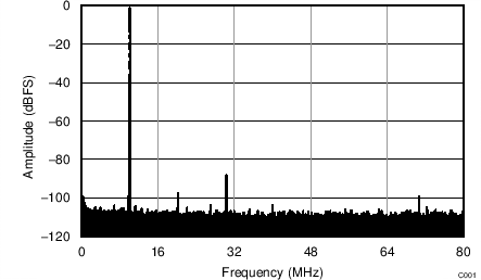
FFT with Dither On
(fS = 160 MSPS, fIN = 10 MHz, SNR = 72.5 dBFS, SFDR = 88 dBc)