SBAS664B May 2014 – November 2014 ADC34J42 , ADC34J43 , ADC34J44 , ADC34J45
PRODUCTION DATA.
- 1 Features
- 2 Applications
- 3 Description
- 4 Revision History
- 5 Device Comparison Table
- 6 Pin Configuration and Functions
-
7 Specifications
- 7.1 Absolute Maximum Ratings
- 7.2 Handling Ratings
- 7.3 Recommended Operating Conditions
- 7.4 Summary of Special Mode Registers
- 7.5 Thermal Information
- 7.6 Electrical Characteristics: ADC34J44, ADC34J45
- 7.7 Electrical Characteristics: ADC34J42, ADC34J43
- 7.8 Electrical Characteristics: General
- 7.9 AC Performance: ADC34J45
- 7.10 AC Performance: ADC34J44
- 7.11 AC Performance: ADC34J43
- 7.12 AC Performance: ADC34J42
- 7.13 Digital Characteristics
- 7.14 Timing Characteristics
- 7.15 Typical Characteristics: ADC34J45
- 7.16 Typical Characteristics: ADC34J44
- 7.17 Typical Characteristics: ADC34J43
- 7.18 Typical Characteristics: ADC34J42
- 7.19 Typical Characteristics: Common Plots
- 7.20 Typical Characteristics: Contour Plots
- 8 Parameter Measurement Information
- 9 Detailed Description
- 10Application and Implementation
- 11Power-Supply Recommendations
- 12Layout
- 13Device and Documentation Support
- 14Mechanical, Packaging, and Orderable Information
Package Options
Mechanical Data (Package|Pins)
- RGZ|48
Thermal pad, mechanical data (Package|Pins)
- RGZ|48
Orderable Information
9 Detailed Description
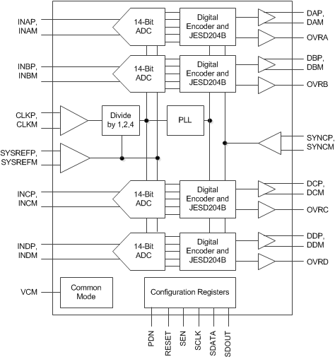
9.1 Overview
The ADC34J4x are a high-linearity, ultra-low power, quad-channel, 14-bit, 50-MSPS to 160-MSPS, analog-to-digital converter (ADC) family. The devices are designed specifically to support demanding, high input frequency signals with large dynamic range requirements. A clock input divider allows more flexibility for system clock architecture design while the SYSREF input enables complete system synchronization. The devices support a JESD204B interface in order to reduce the number of interface lines, thus allowing for high system integration density. The JESD204B interface is a serial interface, where the data of each ADC are serialized and output over only one differential pair. An internal phase-locked loop (PLL) multiplies the incoming ADC sampling clock by 20 to derive the bit clock which is used to serialize the 14-bit data from each channel. The devices support subclass 1 with interface speeds up to 3.2 Gbps.
9.2 Functional Block Diagram
9.3 Feature Description
9.3.1 Analog Inputs
The ADC34J4x analog signal inputs are designed to be driven differentially. Each input pin (INP, INM) must swing symmetrically between (VCM + 0.5 V) and (VCM – 0.5 V), resulting in a 2-VPP (default) differential input swing. The input sampling circuit has a 3-dB bandwidth that extends up to 450 MHz (50-Ω source driving 50-Ω termination between INP and INM).
9.3.2 Clock Input
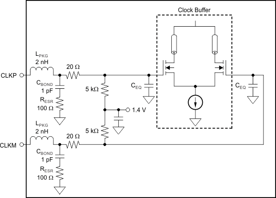
The device clock inputs can be driven differentially (sine, LVPECL, or LVDS) or single-ended (LVCMOS), with little or no difference in performance between them. The common-mode voltage of the clock inputs is set to 1.4 V using internal 5-kΩ resistors. The self-bias clock inputs of the ADC34J4x can be driven by the transformer-coupled, sine-wave clock source or by the ac-coupled, LVPECL and LVDS clock sources, as shown in Figure 148, Figure 149, and Figure 150. See Figure 151 for details regarding the internal clock buffer.
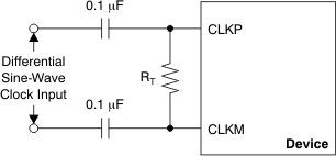
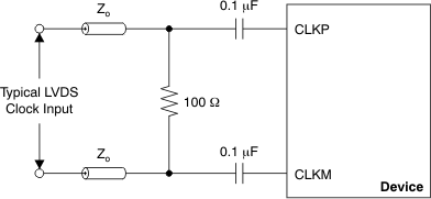 Figure 149. LVDS Clock Driving Circuit
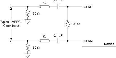 Figure 150. LVPECL Clock Driving Circuit
A single-ended CMOS clock can be ac-coupled to the CLKP input, with CLKM connected to ground with a 0.1-μF capacitor, as shown in Figure 152. However, for best performance the clock inputs must be driven differentially, thereby reducing susceptibility to common-mode noise. For high input frequency sampling, TI recommends using a clock source with very low jitter. Band-pass filtering of the clock source can help reduce the effects of jitter. There is no change in performance with a non-50% duty cycle clock input.
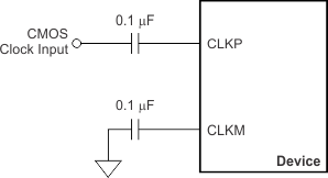 Figure 152. Single-Ended Clock Driving Circuit
9.3.2.1 SNR and Clock Jitter
The signal-to-noise ratio of the ADC is limited by three different factors, as shown in Equation 1. Quantization noise is typically not noticeable in pipeline converters and is 86 dB for a 14-bit ADC. Thermal noise limits SNR at low input frequencies while the clock jitter sets SNR for higher input frequencies.
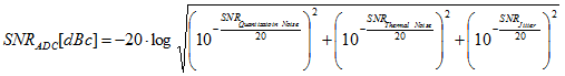
The SNR limitation resulting from sample clock jitter can be calculated with Equation 2:

The total clock jitter (TJitter) has two components: the internal aperture jitter (200 fs for the device) which is set by the noise of the clock input buffer and the external clock. TJitter can be calculated with Equation 3:
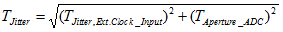
External clock jitter can be minimized by using high-quality clock sources and jitter cleaners as well as band-pass filters at the clock input while a faster clock slew rate improves the ADC aperture jitter. The devices have a thermal noise of 73 dBFS and internal aperture jitter of 200 fs. The SNR, depending on amount of external jitter for different input frequencies, is shown in Figure 153.
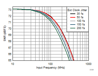 Figure 153. SNR vs Frequency vs Jitter
9.3.2.2 Input Clock Divider
The devices are equipped with an internal divider on the clock input. The divider allows operation with a faster input clock, thus simplifying the system clock distribution design. The clock divider can be bypassed (divide-by-1) for operation with a 160-MHz clock while the divide-by-2 option supports a maximum input clock of 320 MHz and the divide-by-4 option provides a maximum input clock frequency of 640 MHz.
9.3.3 Power-Down Control
The power-down functions of the ADC34J4x can be controlled either through the parallel control pin (PDN) or through an SPI register setting (see register Figure 181, register 15h). The PDN pin can also be configured via SPI to a global power-down or standby functionality, as shown in Table 3.
Table 3. Power-Down Modes
| FUNCTION | POWER CONSUMPTION (mW) | WAKE-UP TIME (µs) |
|---|---|---|
| Global power-down | 5 | 85 |
| Standby | 118 | 35 |
9.3.4 Internal Dither Algorithm
The ADC34J4x uses an internal dither algorithm to achieve high SFDR and a clean spectrum. However, the dither algorithm marginally degrades SNR, creating a trade-off between SNR and SFDR. If desired, the dither algorithm can be turned off by using the DIS DITH CHx registers bits. Figure 154 and Figure 155 show the effect of using dither algorithms.
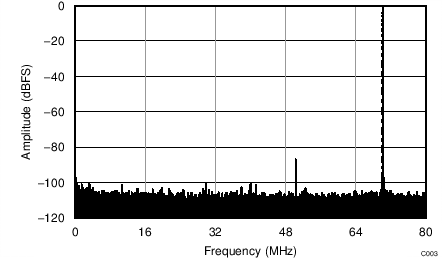
| fS = 160 MSPS, SNR = 71.4 dBFS, fIN = 70 MHz, SFDR = 86 dBc |
||

| fS = 160 MSPS, SNR = 71.8 dBFS, fIN = 70 MHz, SFDR = 85 dBc |
||
9.3.5 JESD204B Interface
The ADC34J4x support device subclass 0, 1, and 2 with a maximum output data rate of 3.2 Gbps for each serial transmitter, as shown in Figure 156. The data of each ADC are serialized by 20x using an internal PLL and then transmitted out on one differential pair each. An external SYSREF (subclass 1) or SYNC (subclass 2) signal is used to align all internal clock phases and the local multiframe clock to a specific sampling clock edge. This process allows synchronization of multiple devices in a system and minimizes timing and alignment uncertainty.
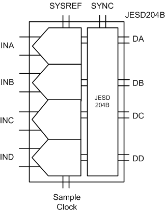 Figure 156. JESD204B Interface
The JESD204B transmitter block consists of the transport layer, the data scrambler, and the link layer, as shown in Figure 157. The transport layer maps the ADC output data into the selected JESD204B frame data format and manages if the ADC output data or test patterns are being transmitted. The link layer performs the 8b/10b data encoding as well as the synchronization and initial lane alignment using the SYNC input signal. Optionally data from the transport layer can be scrambled.
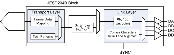 Figure 157. JESD204B Block
9.3.5.1 JESD204B Initial Lane Alignment (ILA)
The initial lane alignment process is started by the receiving device by asserting the SYNC signal. When a logic high is detected on the SYNC input pins, the ADC34J4x starts transmitting comma (K28.5) characters to establish code group synchronization. When synchronization is complete, the receiving device de-asserts the SYNC signal and the ADC34J4x starts the initial lane alignment sequence with the next local multiframe clock boundary. The ADC34J4x transmits four multiframes, each containing K frames (K is SPI programmable). Each multiframe contains the frame start and end symbols; the second multiframe also contains the JESD204 link configuration data.
9.3.5.2 JESD204B Test Patterns
There are three different test patterns available in the transport layer of the JESD204B interface. The ADC34J4x supports a clock output, an encoded, and a PRBS (215 – 1) pattern. These patterns can be enabled via SPI register writes and are located in address 2Ah (bits 7:6).
9.3.5.3 JESD204B Frame Assembly
The JESD204B standard defines the following parameters:
- L is the number of lanes per link,
- M is the number of converters per device,
- F is the number of octets per frame clock period, and
- S is the number of samples per frame.
Table 4. LMFS Values and Interface Rate
| L | M | F | S | MINIMUM ADC SAMPLING RATE (MSPS) | MINIMUM fSERDES (Mbps) | MAXIMUM ADC SAMPLING RATE (Msps) | MAXIMUM fSERDES (GSPS) | MODE |
|---|---|---|---|---|---|---|---|---|
| 4 | 4 | 2 | 1 | 15 | 300 | 160 | 3.2 | 20x (default) |
| 2 | 4 | 4 | 1 | 10 | 400 | 80 | 3.2 | 40x |
The detailed frame assembly for quad-channel mode is shown in Figure 158. The frame assembly configuration can be changed from 20x (default) to 40x by setting the registers listed in Table 5.
 Figure 158. JESD Frame Assembly
Table 5. Configuring 40x Mode
| ADDRESS | DATA |
|---|---|
| 2Bh | 01h |
| 30h | 03h |
9.3.5.4 Digital Outputs
The ADC34J4x JESD204B transmitter uses differential CML output drivers. The CML output current is programmable from 5 mA to 20 mA using SPI register settings. The output driver expects to drive a differential 100-Ω load impedance; place the termination resistors as close to the receiver inputs as possible to avoid unwanted reflections and signal distortion. Because the JESD204B employs 8b, 10b encoding, the output data stream is dc-balanced and ac-coupling can be used avoiding the need to match up common-mode voltages between transmitter and receivers. Connect the termination resistors to the termination voltage as shown in Figure 159.
 Figure 159. CML Output Connections
Figure 160 shows the data eye measurements of the device JESD204B transmitter against the JESD204B transmitter mask at 3.125 Gbps (156.25 MSPS, 20x mode).
 Figure 160. Eye Diagram: 3.125 Gbps
9.4 Device Functional Modes
9.4.1 Digital Gain
The input full-scale amplitude can be selected between 1 VPP to 2 VPP (default is 2 VPP) by choosing the appropriate digital gain setting via an SPI register write. Digital gain provides an option to trade-off SNR for SFDR performance. A larger input full-scale increases SNR performance (2 VPP recommended for maximum SNR) while reduced input swing typically results in better SFDR performance. Table 6 lists the available digital gain settings.
Table 6. Digital Gain vs Full-Scale Amplitude
| DIGITAL GAIN (dB) | MAX INPUT VOLTAGE (VPP) |
|---|---|
| 0 | 2.0 |
| 0.5 | 1.89 |
| 1 | 1.78 |
| 1.5 | 1.68 |
| 2 | 1.59 |
| 2.5 | 1.50 |
| 3 | 1.42 |
| 3.5 | 1.34 |
| 4 | 1.26 |
| 4.5 | 1.19 |
| 5 | 1.12 |
| 5.5 | 1.06 |
| 6 | 1.00 |
9.4.2 Overrange Indication
The ADC34J4x provides two different overrange indications. The normal OVR (default) is triggered if the final 14-bit data output exceeds the maximum code value. The fast OVR is triggered if the input voltage exceeds the programmable overrange threshold and is presented after just nine clock cycles, thus enabling a quicker reaction to an overrange event. By default, the normal overrange indication is output on the OVRx pins (where x is A, B, C, or D). The fast OVR indication can be presented on the overrange pins by using the EN FOVR register bit.
9.5 Programming
The ADC34J4x can be configured using a serial programming interface, as described in this section.
9.5.1 Serial Interface
The device has a set of internal registers that can be accessed by the serial interface formed by the SEN (serial interface enable), SCLK (serial interface clock), SDATA (serial interface data), and SDOUT (serial interface data output) pins. Serially shifting bits into the device is enabled when SEN is low. Serial data SDATA are latched at every SCLK rising edge when SEN is active (low). The serial data are loaded into the register at every 24th SCLK rising edge when SEN is low. When the word length exceeds a multiple of 24 bits, the excess bits are ignored. Data can be loaded in multiples of 24-bit words within a single active SEN pulse. The interface can function with SCLK frequencies from 20 MHz down to very low speeds (of a few hertz) and also with a non-50% SCLK duty cycle.
9.5.1.1 Register Initialization
After power-up, the internal registers must be initialized to their default values through a hardware reset by applying a high pulse on the RESET pin (of durations greater than 10 ns); see Figure 161. If required, the serial interface registers can be cleared during operation either:
- Through a hardware reset, or
- By applying a software reset. When using the serial interface, set the RESET bit (D0 in register address 06h) high. This setting initializes the internal registers to the default values and then self-resets the RESET bit low. In this case, the RESET pin is kept low.
9.5.1.1.1 Serial Register Write
The device internal register can be programmed with these steps:
- Drive the SEN pin low,
- Set the R/W bit to 0 (bit A15 of the 16-bit address),
- Set bit A14 in the address field to 1,
- Initiate a serial interface cycle by specifying the address of the register (A13 to A0) whose content must be written, and
- Write the 8-bit data that are latched in on the SCLK rising edge.
Figure 161 and Table 7 show the timing requirements for the serial register write operation.
 Figure 161. Serial Register Write Timing Diagram
Table 7. Serial Interface Timing(1)
| PARAMETER | MIN | TYP | MAX | UNIT | |
|---|---|---|---|---|---|
| fSCLK | SCLK frequency (equal to 1 / tSCLK) | > dc | 20 | MHz | |
| tSLOADS | SEN to SCLK setup time | 25 | ns | ||
| tSLOADH | SCLK to SEN hold time | 25 | ns | ||
| tDSU | SDIO setup time | 25 | ns | ||
| tDH | SDIO hold time | 25 | ns | ||
9.5.1.1.2 Serial Register Readout
The device includes a mode where the contents of the internal registers can be read back using the SDOUT pin. This readback mode may be useful as a diagnostic check to verify the serial interface communication between the external controller and the ADC. Given below is the procedure to read contents of serial registers:
- Drive the SEN pin low.
- Set the R/W bit (A15) to 1. This setting disables any further writes to the registers.
- Set bit A14 in the address field to 1.
- Initiate a serial interface cycle specifying the address of the register (A13 to A0) whose content must be read.
- The device outputs the contents (D7 to D0) of the selected register on the SDOUT pin.
- The external controller can latch the contents at the SCLK rising edge.
- To enable register writes, reset the R/W register bit to 0.
When READOUT is disabled, the SDOUT pin is in a high-impedance mode. If serial readout is not used, the SDOUT pin must float. Figure 162 shows a timing diagram of the serial register read operation. Data appear on the SDOUT pin at the SCLK falling edge with an approximate delay (tSD_DELAY) of 20 ns, as shown in Figure 163.
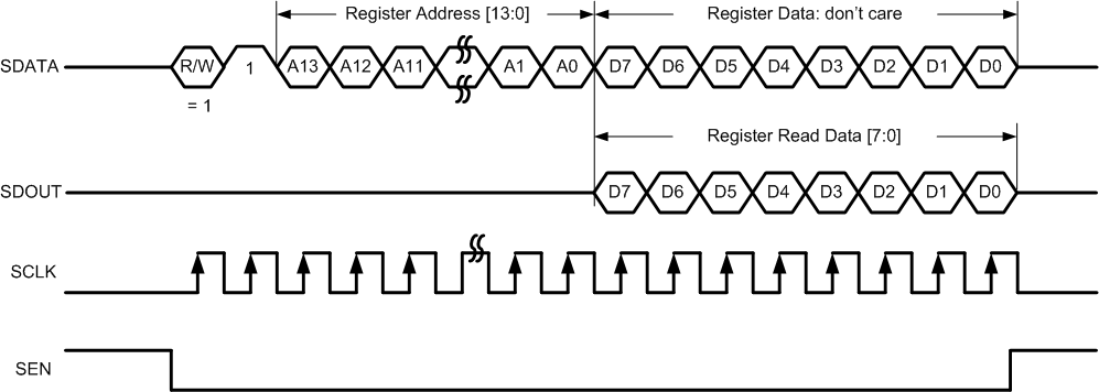 Figure 162. Serial Register Read Timing Diagram
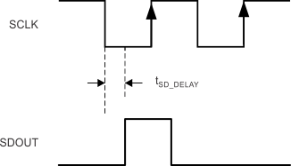 Figure 163. SDOUT Timing Diagram
9.5.2 Register Initialization
After power-up, the internal registers must be initialized to their default values through a hardware reset by applying a high pulse on the RESET pin, as shown in Figure 164 and Table 8.
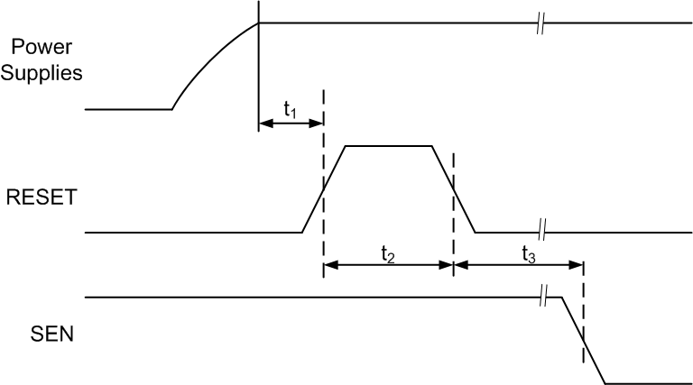 Figure 164. Initialization of Serial Registers after Power-Up
Table 8. Power-Up Timing
| PARAMETER | CONDITIONS | MIN | TYP | MAX | UNIT | |
|---|---|---|---|---|---|---|
| t1 | Power-on delay | Delay from power up to active high RESET pulse | 1 | ms | ||
| t2 | Reset pulse width | Active high RESET pulse width | 10 | 1000 | ns | |
| t3 | Register write delay | Delay from RESET disable to SEN active | 100 | ns | ||
If required, the serial interface registers can be cleared during operation either:
- Through hardware reset, or
- By applying a software reset. When using the serial interface, set the RESET bit (D0 in register address 06h) high. This setting initializes the internal registers to the default values and then self-resets the RESET bit low. In this case, the RESET pin is kept low.
9.5.3 Start-Up Sequence
After power-up, the sequence described in Table 9 can be used to set up the ADC34J4x for basic operation.
Table 9. Start-Up Settings
| STEP | DESCRIPTION | REGISTER ADDRESS AND DATA |
|---|---|---|
| 1 | Supply all supply voltages. There is no required power supply sequence for AVDD and DVDD | — |
| 2 | Pulse hardware reset (low to high to low) on pin 24 | — |
| 3 | Optionally, configure the LMFS of the JESD204B interface in 40x mode, LMFS = 2441 (default is 20x mode, LMFS = 4421) |
Address 2Bh, data 01h Address 30h, data 03h |
| 4 | Pulse SYNC~ from high to low to transmit data from k28.5 sync mode | — |
9.6 Register Map
Table 10. Serial Register Map
| REGISTER ADDRESS | REGISTER DATA | |||||||
|---|---|---|---|---|---|---|---|---|
| A[13:0] (Hex) | 7 | 6 | 5 | 4 | 3 | 2 | 1 | 0 |
| 01 | DIS DITH CHA | DIS DITH CHB | DIS DITH CHC | DIS DITH CHD | ||||
| 02 | 0 | 0 | 0 | 0 | 0 | 0 | CHA GAIN EN | 0 |
| 03 | 0 | 0 | 0 | 0 | 0 | 0 | CHB GAIN EN | 0 |
| 04 | 0 | 0 | 0 | 0 | 0 | 0 | CHC GAIN EN | 0 |
| 05 | 0 | 0 | 0 | 0 | 0 | 0 | CHD GAIN EN | 0 |
| 06 | 0 | 0 | 0 | SPECIAL MODE1 CHA | TEST PATTERN EN | RESET | ||
| 07 | 0 | 0 | 0 | SPECIAL MODE1 CHB | EN FOVR | 0 | ||
| 08 | 0 | 0 | 0 | SPECIAL MODE1 CHC | 0 | 0 | ||
| 09 | 0 | 0 | 0 | SPECIAL MODE1 CHD | ALIGN TEST PATTERN | DATA FORMAT | ||
| 0A | CHA TEST PATTERN | CHB TEST PATTERN | ||||||
| 0B | CHC TEST PATTERN | CHD TEST PATTERN | ||||||
| 0C | CHA DIGITAL GAIN | CHB DIGITAL GAIN | ||||||
| 0D | CHC DIGITAL GAIN | CHD DIGITAL GAIN | ||||||
| 0E | CUSTOM PATTERN (13:6) | |||||||
| 0F | CUSTOM PATTERN (5:0) | 0 | 0 | |||||
| 15 | CHA PDN | CHB PDN | CHC PDN | CHD PDN | STANDBY | GLOBAL PDN | 0 | PDN PIN DISABLE |
| 27 | CLK DIV | 0 | 0 | 0 | 0 | 0 | 0 | |
| 2A | SERDES TEST PATTERN | IDLE SYNC | TRP LAYER TESTMODE EN | FLIP ADC DATA | LANE ALIGN | FRAME ALIGN | TXMIT LINKDATA DIS | |
| 2B | 0 | 0 | 0 | 0 | 0 | 0 | CTRL K | CTRL F |
| 2F | SCR (SCR EN) | 0 | 0 | 0 | 0 | 0 | 0 | 0 |
| 30 | OCTETS PER FRAME | |||||||
| 31 | 0 | 0 | 0 | FRAMES PER MULTI FRAME | ||||
| 34 | SUBCLASSV | 0 | 0 | 0 | 0 | 0 | ||
| 3A | SYNC REQ | OPTION SYNC REG | 0 | 0 | OUTPUT CURRENT SEL | 0 | ||
| 3B | LINK LAYER TESTMODE SEL[2:0] | LINK LAYER RPAT | 0 | PULSE DET MODES | ||||
| 3C | FORCE LMFC COUNT | LMFC COUNT INIT | LMFC COUNT INIT | |||||
| 122 | 0 | 0 | 0 | 0 | 0 | 0 | SPECIAL MODE2 CHA [1:0] |
|
| 134 | 0 | 0 | DIS DITH CHA | 0 | DIS DITH CHA | 0 | 0 | 0 |
| 222 | 0 | 0 | 0 | 0 | 0 | 0 | SPECIAL MODE2 CHD [1:0] |
|
| 234 | 0 | 0 | DIS DITH CHD | 0 | DIS DITH CHD | 0 | 0 | 0 |
| 422 | 0 | 0 | 0 | 0 | 0 | 0 | SPECIAL MODE2 CHB [1:0] |
|
| 434 | 0 | 0 | DIS DITH CHB | 0 | DIS DITH CHB | 0 | 0 | 0 |
| 522 | 0 | 0 | 0 | 0 | 0 | 0 | SPECIAL MODE2 CHC [1:0] |
|
| 534 | 0 | 0 | DIS DITH CHC | 0 | DIS DITH CHC | 0 | 0 | 0 |
9.6.1 Serial Register Description
| 7 | 6 | 5 | 4 | 3 | 2 | 1 | 0 |
| DIS DITH CHA | DIS DITH CHB | DIS DITH CHC | DIS DITH CHD | ||||
Table 11. Register 01h Description
| Name | Description |
|---|---|
| Bits 7:6 | DIS DITH CHA |
| 00 = Default 11 = Dither is disabled, high SNR mode is selected for channel A. In this mode, SNR typically improves by 0.5 dB at 70 MHz. Ensure that register 134 (bits 5 and 3) are also set to 11. |
|
| Bits 5:4 | DIS DITH CHB |
| 00 = Default 11 = Dither is disabled, high SNR mode is selected for channel B. In this mode, SNR typically improves by 0.5 dB at 70 MHz. Ensure that register 434 (bits 5 and 3) are also set to 11. |
|
| Bits 3:2 | DIS DITH CHC |
| 00 = Default 11 = Dither is disabled, high SNR mode is selected for channel C. In this mode, SNR typically improves by 0.5 dB at 70 MHz. Ensure that register 534 (bits 5 and 3) are also set to 11. |
|
| Bits 1:0 | DIS DITH CHD |
| 00 = Default 11 = Dither is disabled, high SNR mode is selected for channel D. In this mode, SNR typically improves by 0.5 dB at 70 MHz. Ensure that register 234 (bits 5 and 3) are also set to 11. |
| 7 | 6 | 5 | 4 | 3 | 2 | 1 | 0 |
| 0 | 0 | 0 | 0 | 0 | 0 | CHA GAIN EN | 0 |
Table 12. Register 02h Description
| Name | Description |
|---|---|
| Bits 7:2 | Must write 0 |
| Bit 1 | CHA GAIN EN |
| Enable digital gain control for channel A. 0 = Default 1 = Digital gain for channel A can be programmed with the CHA DIGITAL GAIN bits. |
|
| Bit 0 | Must write 0 |
| 7 | 6 | 5 | 4 | 3 | 2 | 1 | 0 |
| 0 | 0 | 0 | 0 | 0 | 0 | CHB GAIN EN | 0 |
Table 13. Register 03h Description
| Name | Description |
|---|---|
| Bits 7:2 | Must be 0 |
| Bit 1 | CHB GAIN EN: |
| Enable digital gain control for channel B. 0 = Default 1 = Digital gain for channel B can be programmed with the CHB DIGITAL GAIN bits. |
|
| Bit 0 | Must write 0 |
| 7 | 6 | 5 | 4 | 3 | 2 | 1 | 0 |
| 0 | 0 | 0 | 0 | 0 | 0 | CHC GAIN EN | 0 |
Table 14. Register 04h Description
| Name | Description |
|---|---|
| Bits 7:2 | Must write 0 |
| Bit 1 | CHC GAIN EN |
| Enable digital gain control for channel C. 0 = Default 1 = Digital gain for channel C can be programmed with the CHC DIGITAL GAIN bits. |
|
| Bit 0 | Must write 0 |
| 7 | 6 | 5 | 4 | 3 | 2 | 1 | 0 |
| 0 | 0 | 0 | 0 | 0 | 0 | CHD GAIN EN | 0 |
Table 15. Register 05h Description
| Name | Description |
|---|---|
| Bits 7:2 | Must write 0 |
| Bit 1 | CHD GAIN EN: |
| Enable digital gain control for channel D 0 = Default 1 = Digital gain for channel D can be programmed with the CHD DIGITAL GAIN bits. |
|
| Bit 0 | Must write 0 |
| 7 | 6 | 5 | 4 | 3 | 2 | 1 | 0 |
| 0 | 0 | 0 | SPECIAL MODE1 CHA | TEST PATTERN EN | RESET | ||
Table 16. Register 06h Description
| Name | Description |
|---|---|
| Bits 7:5 | Must write 0 |
| Bits 4:2 | SPECIAL MODE1 CHA |
| 010 = For frequencies < 120 MHz 111 = For frequencies > 120 MHz |
|
| Bit 1 | TEST PATTERN EN |
| This bit enables test pattern selection for the digital outputs. 0 = Normal operation 1 = Test pattern output enabled |
|
| Bit 0 | RESET: Software reset applied |
| This bit resets all internal registers to the default values and self-clears to 0. |
| 7 | 6 | 5 | 4 | 3 | 2 | 1 | 0 |
| 0 | 0 | 0 | SPECIAL MODE1 CHB | EN FOVR | 0 | ||
Table 17. Register 07h Description
| Name | Description |
|---|---|
| Bits 7:5 | Must write 0 |
| Bits 4:2 | SPECIAL MODE1 CHB |
| 010 = For frequencies < 120 MHz 111 = For frequencies > 120 MHz |
|
| Bit 1 | EN FOVR |
| 0 = Normal OVR on OVRx pins 1 = Enable fast OVR on OVRx pins |
|
| Bit 0 | Must write 0 |
| 7 | 6 | 5 | 4 | 3 | 2 | 1 | 0 |
| 0 | 0 | 0 | SPECIAL MODE1 CHC | 0 | 0 | ||
Table 18. Register 08h Description
| Name | Description |
|---|---|
| Bits 7:5 | Must write 0 |
| Bits 4:2 | SPECIAL MODE1 CHC |
| 010 = For frequencies < 120 MHz 111 = For frequencies > 120 MHz |
|
| Bits 1:0 | Must write 0 |
| 7 | 6 | 5 | 4 | 3 | 2 | 1 | 0 |
| 0 | 0 | 0 | SPECIAL MODE1 CHD | ALIGN TEST PATTERN | DATA FORMAT | ||
Table 19. Register 09h Description
| Name | Description |
|---|---|
| Bits 7:5 | Must write 0 |
| Bits 4:2 | SPECIAL MODE1 CHD |
| 010 = For frequencies < 120 MHz 111 = For frequencies > 120 MHz |
|
| Bit 1 | ALIGN TEST PATTERN |
| This bit aligns test patterns across the outputs of four channels. 0 = Test patterns of four channels are free running. 1 = Test patterns of four channels are aligned. |
|
| Bit 0 | DATA FORMAT: Digital output data format |
| 0 = Twos complement 1 = Offset binary |
| 7 | 6 | 5 | 4 | 3 | 2 | 1 | 0 |
| CHA TEST PATTERN | CHB TEST PATTERN | ||||||
Table 20. Register 0Ah Description
| Name | Description |
|---|---|
| Bits 7:4 | CHA TEST PATTERN |
| These bits control the test pattern for channel A after the TEST PATTERN EN bit is set. 0000 = Normal operation 0001 = All 0's 0010 = All 1's 0011 = Toggle pattern: data alternate between 10101010101010 and 01010101010101. 0100 = Digital ramp: data increment by 1 LSB every clock cycle from code 0 to 16383. 0101 = Custom pattern: output data are the same as programmed by the CUSTOM PATTERN register bits. 0110 = Deskew pattern: data are 3AAAh. 1000 = PRBS pattern: data are a sequence of pseudo random numbers. 1001 = 8-point sine wave: data are a repetitive sequence of the following eight numbers that form a sine-wave: 0, 2399, 8192, 13984, 16383, 13984, 8192, 2399. Others = Do not use |
|
| Bits 3:0 | CHB TEST PATTERN |
| These bits control the test pattern for channel B after the TEST PATTERN EN bit is set. 0000 = Normal operation 0001 = All 0's 0010 = All 1's 0011 = Toggle pattern: data alternate between 10101010101010 and 01010101010101. 0100 = Digital ramp: data increment by 1 LSB every clock cycle from code 0 to 16383. 0101= Custom pattern: output data are the same as programmed by the CUSTOM PATTERN register bits. 0110 = Deskew pattern: data are 3AAAh. 1000 = PRBS pattern: data are a sequence of pseudo random numbers. 1001 = 8-point sine wave: data are a repetitive sequence of the following eight numbers that form a sine-wave: 0, 2399, 8192, 13984, 16383, 13984, 8192, 2399. Others = Do not use |
| 7 | 6 | 5 | 4 | 3 | 2 | 1 | 0 |
| CHC TEST PATTERN | CHD TEST PATTERN | ||||||
Table 21. Register 0Bh Description
| Name | Description |
|---|---|
| Bits 7:4 | CHC TEST PATTERN |
| These bits control the test pattern for channel C after the TEST PATTERN EN bit is set. 0000 = Normal operation 0001 = All 0's 0010 = All 1's 0011 = Toggle pattern: data alternate between 10101010101010 and 01010101010101. 0100 = Digital ramp: data increment by 1 LSB every clock cycle from code 0 to 16383. 0101= Custom pattern: output data are the same as programmed by the CUSTOM PATTERN register bits. 0110 = Deskew pattern: data are 3AAAh. 1000 = PRBS pattern: data are a sequence of pseudo random numbers. 1001 = 8-point sine wave: data are a repetitive sequence of the following eight numbers that form a sine-wave: 0, 2399, 8192, 13984, 16383, 13984, 8192, 2399. Others = Do not use |
|
| Bits 3:0 | CHD TEST PATTERN |
| These bits control the test pattern for channel D after the TEST PATTERN EN bit is set. 0000 = Normal operation 0001 = All 0's 0010 = All 1's 0011 = Toggle pattern: data alternate between 10101010101010 and 01010101010101. 0100 = Digital ramp: data increment by 1 LSB every clock cycle from code 0 to 16383. 0101= Custom pattern: output data are the same as programmed by the CUSTOM PATTERN register bits. 0110 = Deskew pattern: data are 3AAAh. 1000 = PRBS pattern: data are a sequence of pseudo random numbers. 1001 = 8-point sine wave: data are a repetitive sequence of the following eight numbers that form a sine-wave: 0, 2399, 8192, 13984, 16383, 13984, 8192, 2399. Others = Do not use |
| 7 | 6 | 5 | 4 | 3 | 2 | 1 | 0 |
| CHA TEST PATTERN | CHB TEST PATTERN | ||||||
Table 22. Register 0Ch Description
| Name | Description |
|---|---|
| Bits 7:4 | CHA TEST PATTERN |
| In address 0Ch, these bits control the test pattern for channel A after the CHA GAIN EN bit is set. See Table 23 for register settings. | |
| Bits 3:0 | CHB TEST PATTERN |
| In address 0Ch, these bits control the test pattern for channel B after the CHB GAIN EN bit is set. See Table 23 for register settings. |
Table 23. Channel Digital Gain
| REGISTER VALUE | DIGITAL GAIN (dB) | MAXIMUM INPUT VOLTAGE (VPP) |
|---|---|---|
| 0000 | 0 | 2.0 |
| 0001 | 0.5 | 1.89 |
| 0010 | 1 | 1.78 |
| 0011 | 1.5 | 1.68 |
| 0100 | 2 | 1.59 |
| 0101 | 2.5 | 1.50 |
| 0110 | 3 | 1.42 |
| 0111 | 3.5 | 1.34 |
| 1000 | 4 | 1.26 |
| 1001 | 4.5 | 1.19 |
| 1010 | 5 | 1.12 |
| 1011 | 5.5 | 1.06 |
| 1100 | 6 | 1.00 |
| 7 | 6 | 5 | 4 | 3 | 2 | 1 | 0 |
| CHC TEST PATTERN | CHD TEST PATTERN | ||||||
Table 24. Register 0Dh Description
| Name | Description |
|---|---|
| Bits 7:4 | CHC TEST PATTERN |
| In address 0Dh, these bits control the test pattern for channel C after the CHC GAIN EN bit is set. See Table 23 for register settings. | |
| Bits 3:0 | CHD TEST PATTERN |
| In address 0Dh, these bits control the test pattern for channel D after the CHD GAIN EN bit is set. See Table 23 for register settings. |
| 7 | 6 | 5 | 4 | 3 | 2 | 1 | 0 |
| CUSTOM PATTERN (13:6) | |||||||
Table 25. Register 0Eh Description
| Name | Description |
|---|---|
| Bits 7:0 | CUSTOM PATTERN (13:6) |
| These bits set the 14-bit custom pattern (13:6) for all channels. |
| 7 | 6 | 5 | 4 | 3 | 2 | 1 | 0 |
| CUSTOM PATTERN (5:0) | 0 | 0 | |||||
Table 26. Register 0Fh Description
| Name | Description |
|---|---|
| Bits 7:2 | CUSTOM PATTERN (5:0) |
| These bits set the 14-bit custom pattern (5:0) for all channels. | |
| Bits 1:0 | Must write 0 |
| 7 | 6 | 5 | 4 | 3 | 2 | 1 | 0 |
| LOW SPEED MODE | 0 | 0 | 0 | 0 | 0 | 0 | 0 |
Table 27. Register 13h Description
| Name | Description |
|---|---|
| Bit 7 | LOW SPEED MODE |
| Use this bit for sampling frequencies < 25 MSPS. 0 = Normal operation 1 = Low-speed mode enabled |
|
| Bits 6:0 | Must write 0 |
| 7 | 6 | 5 | 4 | 3 | 2 | 1 | 0 |
| CHA PDN | CHB PDN | CHC PDN | CHD PDN | STANDBY | GLOBAL PDN | 0 | CONFIG PDN PIN |
Table 28. Register 15h Description
| Name | Description |
|---|---|
| Bit 7 | CHA PDN: Power-down channel A |
| 0 = Normal operation 1 = Power-down channel A |
|
| Bit 6 | CHB PDN: Power-down channel B |
| 0 = Normal operation 1 = Power-down channel B |
|
| Bit 5 | CHC PDN: Power-down channel C |
| 0 = Normal operation 1 = Power-down channel C |
|
| Bit 4 | CHD PDN: Power-down channel D |
| 0 = Normal operation 1 = Power-down channel D |
|
| Bit 3 | STANDBY |
| This bit places the ADCs of all four channels into standby. 0 = Normal operation 1 = Standby |
|
| Bit 2 | GLOBAL PDN |
| Places device in global power down. 0 = Normal operation 1 = Global power-down |
|
| Bit 1 | Must write 0 |
| Bit 0 | CONFIG PDN PIN |
| This bit configures the PDN pin as either global power-down or standby pin. 0 = Logic high voltage on the PDN pin sends places the into global power-down. 1 = Logic high voltage on the PDN pin places the device into standby. |
| 7 | 6 | 5 | 4 | 3 | 2 | 1 | 0 |
| CLK DIV | 0 | 0 | 0 | 0 | 0 | 0 | |
Table 29. Register 27h Description
| Name | Description |
|---|---|
| Bits 7:6 | CLK DIV: Internal clock divider for the input sampling clock |
| 00 = Clock divider bypassed 01 = Divide-by-1 10 = Divide-by-2 11 = Divide-by-4 |
|
| Bits 5:0 | Must write 0 |
| 7 | 6 | 5 | 4 | 3 | 2 | 1 | 0 |
| SERDES TEST PATTERN | IDLE SYNC | TESTMODE EN | FLIP ADC DATA | LANE ALIGN | FRAME ALIGN | TX LINK CONFIG DATA DIS | |
Table 30. Register 2Ah Description
| Name | Description |
|---|---|
| Bits 7:6 | SERDES TEST PATTERN: |
| These bits set the test patterns in the transport layer of the JESD204B interface. 00 = Normal operation 01 = Outputs clock pattern (output is 10101010) 10 = Encoded pattern (output is 1111111100000000) 11 = Output is 215 – 1 |
|
| Bit 5 | IDLE SYNC |
| This bit generates the long transport layer test pattern mode according to 5.1.6.3 clause of JESD204B specification. 0 = Test mode disabled 1 = Test mode enabled |
|
| Bit 4 | TESTMODE EN |
| This bit sets the output pattern when SYNC is high. 0 = Sync code is k28.5 (0xBCBC) 1 = Sync code is 0xBC50 |
|
| Bit 3 | FLIP ADC DATA |
| This bit sets the output pattern when SYNC is high. 0 = Normal operation 1 = Output data order is reversed: MSB – LSB |
|
| Bit 2 | LANE ALIGN |
| This bit inserts a lane alignment character (K28.3) for the receiver to align to the lane boundary per section 5.3.3.5 of the JESD204B specification. 0 = Normal operation 1 = Inserts lane alignment characters |
|
| Bit 1 | FRAME ALIGN |
| This bit inserts a frame alignment character (K28.7) for the receiver to align to the frame boundary per section 5.3.3.4 of the JESD204B specification. 0 = Normal operation 1 = Inserts frame alignment characters |
|
| Bit 0 | TX LINK CONFIG DATA DIS |
| This bit disables the initial link alignment (ILA) sequence when SYNC is de-asserted. 0 = Normal operation 1 = ILA disabled |
| 7 | 6 | 5 | 4 | 3 | 2 | 1 | 0 |
| 0 | 0 | 0 | 0 | 0 | 0 | CTRL K | CTRL F |
Table 31. Register 2Bh Description
| Name | Description |
|---|---|
| Bits 7:2 | Must write 0 |
| Bit 1 | CTRL K: Enable bit for number of frames per multiframe |
| 0 = Default is 9 frames (20x mode) per multiframe 1 = Frames per multiframe can be set in register 31h |
|
| Bit 0 | CTRL F: Enable bit for number of octets per frame |
| 0 = 20x mode using one lane per ADC (default is F = 2) 1 = Octets per frame can be specified in register 30h |
| 7 | 6 | 5 | 4 | 3 | 2 | 1 | 0 |
| SCRAMBLE EN | 0 | 0 | 0 | 0 | 0 | 0 | 0 |
Table 32. Register 2Fh Description
| Name | Description |
|---|---|
| Bit 7 | SCRAMBLE EN |
| This bit scrambles the enable bit in the JESD204B interface. 0 = Scrambling disabled 1 = Scrambling enabled |
|
| Bits 6:0 | Must write 0 |
| 7 | 6 | 5 | 4 | 3 | 2 | 1 | 0 |
| OCTETS PER FRAME | |||||||
Table 33. Register 30h Description
| Name | Description |
|---|---|
| Bits 7:0 | OCTETS PER FRAME |
| These bits set the number of octets per frame (F). 00000000 = 20x serialization: two octets per frame 00000011 = 40x serialization: four octets per frame |
| 7 | 6 | 5 | 4 | 3 | 2 | 1 | 0 |
| 0 | 0 | 0 | FRAMES PER MULTI FRAME | ||||
Table 34. Register 31h Description
| Name | Description |
|---|---|
| Bits 7:5 | Must write 0 |
| Bits 4:0 | FRAMES PER MULT IFRAME |
| These bits set the number of frames per multiframe. After reset, the default settings for frames per multiframe are: 20x mode: K = 8 (for each mode, do not set K to a lower value). |
| 7 | 6 | 5 | 4 | 3 | 2 | 1 | 0 |
| SUBCLASS | 0 | 0 | 0 | 0 | 0 | ||
Table 35. Register 34h Description
| Name | Description |
|---|---|
| Bits 7:5 | SUBCLASS |
| These bits set the JESD204B subclass. 000 = Subclass 0 (backward compatibility with JESD204A) 001 = Subclass 1 (deterministic latency using SYSREF signal) 010 = Subclass 2 (deterministic latency using SYNC detection) |
|
| Bits 4:0 | Must write 0 |
| 7 | 6 | 5 | 4 | 3 | 2 | 1 | 0 |
| SYNC REQ | SYNC REQ EN | 0 | 0 | OUTPUT CURRENT SEL | 0 | ||
Table 36. Register 3Ah Description
| Name | Description | |
|---|---|---|
| Bit 7 | SYNC REQ | |
| This bit generates a synchronization request only when the SYNC REQ EN register bit is set. 0 = Normal operation 1 = Generates sync request |
||
| Bit 6 | SYNC REQ EN | |
| 0 = Sync request is made with the SYNCP~, SYNCM~ pins 1 = Sync request is made with the SYNC REQ register bit |
||
| Bits 5:4 | Must write 0 | |
| Bits 3:1 | OUTPUT CURRENT SEL: JESD output buffer current selection | |
| Program current (mA) 000 =16 001 = 12 010 = 8 011 = 4 100 = 32 101 = 28 110 = 24 111 = 20 |
||
| Bit 0 | Must write 0 | |
| 7 | 6 | 5 | 4 | 3 | 2 | 1 | 0 |
| LINK LAYER TESTMODE | LINK LAYER RPAT | 0 | PULSE DET MODES | ||||
Table 37. Register 3Bh Description
| Name | Description |
|---|---|
| Bits 7:5 | LINK LAYER TESTMODE |
| These bits generate a pattern according to clause 5.3.3.8.2 of the JESD204B document. 000 = Normal ADC data 001 = D21.5 (high frequency jitter pattern) 010 = K28.5 (mixed frequency jitter pattern) 011 = Repeat initial lane alignment (generates K28.5 character and repeat lane alignment sequences continuously) 100 = 12 octet RPAT jitter pattern |
|
| Bit 4 | LINK LAYER RPAT |
| This bit changes the running disparity in the modified RPAT pattern test mode (only when link layer test mode = 100). 0 = normal operation 1 = changes disparity |
|
| Bit 3 | Must write 0 |
| Bits 2:0 | PULSE DET MODES |
| These bits select different detection modes for SYSREF (subclass 1) and SYNC (subclass2). |
Table 38. PULSE DET MODES Register Settings
| D2 | D1 | D0 | FUNCTIONALITY |
| 0 | Don’t care | 0 | Allow all pulses to reset input clock dividers |
| 1 | Don’t care | 0 | Do not allow reset of analog clock dividers |
| Don’t care | 0 to 1 transition | 1 | Allow one pulse immediately after the 0 to1 transition to reset the divider |
| 7 | 6 | 5 | 4 | 3 | 2 | 1 | 0 |
| FORCE LMFC COUNT | LMFC COUNT INIT | RELEASE ILANE SEQ | |||||
Table 39. Register 3Ch Description
| Name | Description |
|---|---|
| Bit 7 | FORCE LMFC COUNT: Force LMFC count |
| 0 = Normal operation 1 = Enables using different starting values for the LMFC counter |
|
| Bits 6:2 | LMFC COUNT INIT |
| If SYSREF is transmitted to the digital block, the LMFC count resets to 0 and K28.5 stops transmitting when the LMFC count reaches 31. The initial value that the LMFC count resets to can be set using LMFC COUNT INIT. In this manner, the Rx can be synchronized early because the Rx receives the LANE ALIGNMENT SEQUENCE early. The FORCE LMFC COUNT register bit must be enabled. | |
| Bits 1:0 | RELEASE ILANE SEQ |
| These bits delay the lane alignment sequence generation by 0, 1, 2, or 3 multiframes after the code group synchronization. 00 = 0 01 = 1 10 = 2 11 = 3 |
| 7 | 6 | 5 | 4 | 3 | 2 | 1 | 0 |
| 0 | 0 | 0 | 0 | 0 | 0 | SPECIAL MODE2 CHA [1:0] |
|
Table 40. Register 122h Description
| Name | Description |
|---|---|
| Bits 7:2 | Must write 0 |
| Bit 1:0 | SPECIAL MODE2 CHA [1:0] |
| Always write 1 for better HD2 performance. |
| 7 | 6 | 5 | 4 | 3 | 2 | 1 | 0 |
| 0 | 0 | DIS DITH CHA | 0 | DIS DITH CHA | 0 | 0 | 0 |
Table 41. Register 134h Description
| Name | Description |
|---|---|
| Bits 7:6 | Must write 0 |
| Bit 5 | DIS DITH CHA |
| 00 = Default 11 = Dither is disabled and high SNR mode is selected for channel A. In this mode, SNR typically improves by 0.5 dB at 70 MHz. Ensure that register 01h (bits 3:2) are also set to 11. |
|
| Bit 4 | Must write 0 |
| Bit 3 | DIS DITH CHA |
| 00 = Default 11 = Dither is disabled and high SNR mode is selected for channel A. In this mode, SNR typically improves by 0.5 dB at 70 MHz. Ensure that register 01h (bits 3:2) are also set to 11. |
|
| Bits 2:0 | Must write 0 |
| 7 | 6 | 5 | 4 | 3 | 2 | 1 | 0 |
| 0 | 0 | 0 | 0 | 0 | 0 | SPECIAL MODE2 CHD [1:0] |
0 |
Table 42. Register 222h Description
| Name | Description |
|---|---|
| Bits 7:2 | Must write 0 |
| Bit 1:0 | SPECIAL MODE2 CHD [1:0] |
| Always write 1 for better HD2 performance. |
| 7 | 6 | 5 | 4 | 3 | 2 | 1 | 0 |
| 0 | 0 | DIS DITH CHD | 0 | DIS DITH CHD | 0 | 0 | 0 |
Table 43. Register 234h Description
| Name | Description |
|---|---|
| Bits 7:6 | Must write 0 |
| Bit 5 | DIS DITH CHD |
| 00 = Default 11 = Dither is disabled and high SNR mode is selected for channel D. In this mode, SNR typically improves by 0.5 dB at 70 MHz. Ensure that register 01h (bits 3:2) are also set to 11. |
|
| Bit 4 | Must write 0 |
| Bit 3 | DIS DITH CHD |
| 00 = Default 11 = Dither is disabled and high SNR mode is selected for channel D. In this mode, SNR typically improves by 0.5 dB at 70 MHz. Ensure that register 01h (bits 3:2) are also set to 11. |
|
| Bits 2:0 | Must write 0 |
| 7 | 6 | 5 | 4 | 3 | 2 | 1 | 0 |
| 0 | 0 | 0 | 0 | 0 | 0 | SPECIAL MODE2 CHB [1:0] |
0 |
Table 44. Register 422h Description
| Name | Description |
|---|---|
| Bits 7:2 | Must write 0 |
| Bit 1:0 | SPECIAL MODE2 CHB [1:0] |
| Always write 1 for better HD2 performance. |
| 7 | 6 | 5 | 4 | 3 | 2 | 1 | 0 |
| 0 | 0 | DIS DITH CHB | 0 | DIS DITH CHB | 0 | 0 | 0 |
Table 45. Register 434h Description
| Name | Description |
|---|---|
| Bits 7:6 | Must write 0 |
| Bit 5 | DIS DITH CHB |
| 00 = Default 11 = Dither is disabled and high SNR mode is selected for channel B. In this mode, SNR typically improves by 0.5 dB at 70 MHz. Ensure that register 01h (bits 3:2) are also set to 11. |
|
| Bit 4 | Must write 0 |
| Bit 3 | DIS DITH CHB |
| 00 = Default 11 = Dither is disabled and high SNR mode is selected for channel B. In this mode, SNR typically improves by 0.5 dB at 70 MHz. Ensure that register 01h (bits 3:2) are also set to 11. |
|
| Bits 2:0 | Must write 0 |
| 7 | 6 | 5 | 4 | 3 | 2 | 1 | 0 |
| 0 | 0 | 0 | 0 | 0 | 0 | SPECIAL MODE2 CHC [1:0] |
0 |
Table 46. Register 522h Description
| Name | Description |
|---|---|
| Bits 7:2 | Must write 0 |
| Bit 1:0 | SPECIAL MODE2 CHC [1:0] |
| Always write 1 for better HD2 performance. |
| 7 | 6 | 5 | 4 | 3 | 2 | 1 | 0 |
| 0 | 0 | DIS DITH CHC | 0 | DIS DITH CHC | 0 | 0 | 0 |
Table 47. Register 534h Description
| Name | Description |
|---|---|
| Bits 7:6 | Must write 0 |
| Bit 5 | DIS DITH CHC |
| 00 = Default 11 = Dither is disabled and high SNR mode is selected for channel C. In this mode, SNR typically improves by 0.5 dB at 70 MHz. Ensure that register 01h (bits 3:2) are also set to 11. |
|
| Bit 4 | Must write 0 |
| Bit 3 | DIS DITH CHC |
| 00 = Default 11 = Dither is disabled and high SNR mode is selected for channel C. In this mode, SNR typically improves by 0.5 dB at 70 MHz. Ensure that register 01h (bits 3:2) are also set to 11. |
|
| Bits 2:0 | Must write 0 |