SBAS480C september   2009  – june 2023 ADS1000-Q1

PRODUCTION DATA  

  1.   1
  2. Features
  3. Applications
  4. Description
  5. Revision History
  6. Pin Configuration and Functions
  7. Specifications
    1. 6.1 Absolute Maximum Ratings
    2. 6.2 ESD Ratings
    3. 6.3 Recommended Operating Conditions
    4. 6.4 Thermal Information
    5. 6.5 Electrical Characteristics
    6. 6.6 Timing Requirements
    7. 6.7 Timing Diagram
    8. 6.8 Typical Characteristics
  8. Detailed Description
    1. 7.1 Overview
    2. 7.2 Functional Block Diagram
    3. 7.3 Feature Description
      1. 7.3.1 Analog-to-Digital Converter
      2. 7.3.2 Clock Generator
    4. 7.4 Device Functional Modes
      1. 7.4.1 Operating Modes
      2. 7.4.2 Reset and Power Up
    5. 7.5 Programming
      1. 7.5.1 I2C Interface
      2. 7.5.2 ADS1000-Q1 I2C Addresses
      3. 7.5.3 I2C General Call
      4. 7.5.4 I2C Data Rates
      5. 7.5.5 Output Code Calculation
    6. 7.6 Register Maps
      1. 7.6.1 Output Register
      2. 7.6.2 Configuration Register
      3. 7.6.3 Reading From the ADS1000-Q1
      4. 7.6.4 Writing to the ADS1000-Q1
  9. Application and Implementation
    1. 8.1 Application Information
      1. 8.1.1 Basic Connections
        1. 8.1.1.1 Connecting Multiple Devices
        2. 8.1.1.2 Using GPIO Ports For I2C
        3. 8.1.1.3 Single-Ended Inputs
    2. 8.2 Typical Applications
      1. 8.2.1 ADS1000-Q1 With Current-Shunt Monitor
        1. 8.2.1.1 Design Requirements
        2. 8.2.1.2 Detailed Design Procedure
          1. 8.2.1.2.1 Part Selection
            1. 8.2.1.2.1.1 Gain Settings
            2. 8.2.1.2.1.2 Circuit Implementation
        3. 8.2.1.3 Application Curve
      2. 8.2.2 Low-Side Current Measurement
        1. 8.2.2.1 Design Requirements
        2. 8.2.2.2 Detailed Design Procedure
    3. 8.3 Power Supply Recommendations
    4. 8.4 Layout
      1. 8.4.1 Layout Guidelines
      2. 8.4.2 Layout Example
  10. Device and Documentation Support
    1. 9.1 Receiving Notification of Documentation Updates
    2. 9.2 Support Resources
    3. 9.3 Trademarks
    4. 9.4 Electrostatic Discharge Caution
    5. 9.5 Glossary
  11. 10Mechanical, Packaging, and Orderable Information

Package Options

Mechanical Data (Package|Pins)
Thermal pad, mechanical data (Package|Pins)
Orderable Information

Reading From the ADS1000-Q1

The output register and the contents of the configuration register can be read from the ADS1000-Q1. To read data, address the ADS1000-Q1 for reading, and read three bytes from the device. The first two bytes are the output register contents; the third byte is the configuration register contents.

Three bytes do not always have to read from the ADS1000-Q1. If only the contents of the output register are needed, read only two bytes.

Reading more than three bytes from the ADS1000-Q1 has no effect. All bytes beginning with the fourth byte are FFh. Figure 7-3 shows a timing diagram of an ADS1000-Q1 read operation.
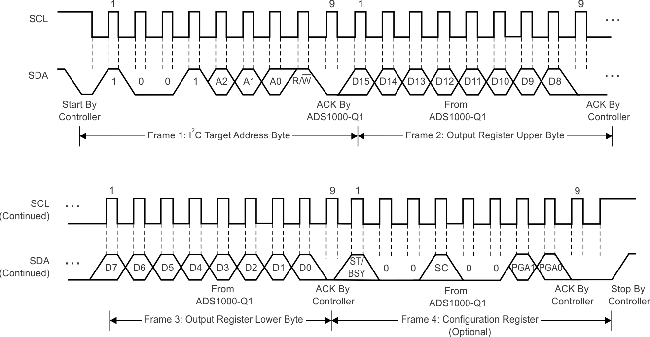
GUID-0B5DF2C5-42B6-4C27-8E7F-4098C9FEA3DC-low.gif Figure 7-3 Timing Diagram for Reading from the ADS1000-Q1